Wedoany.com Report on Feb 7th, The global chip manufacturing giant Taiwan Semiconductor Manufacturing Company (TSMC) officially announced on Thursday that its second wafer fabrication plant currently under construction in Kumamoto Prefecture, Japan (referred to as "Kumamoto Fab 2") will incorporate one of the industry's most advanced semiconductor manufacturing technologies—the 3-nanometer process—for producing high-performance chips. These chips are core components that drive the operation of artificial intelligence systems, high-performance computing, and next-generation consumer electronic devices.
As the world's largest dedicated semiconductor foundry, TSMC's products are widely used in various critical devices ranging from smartphones to AI servers. The company had previously built and commenced operations at its first factory in Kumamoto (mainly producing 22/28nm and 12/16nm chips). This expansion and upgrade of the second factory aim to further strengthen its production capacity layout in Japan and the Asian region, enhancing the resilience and stability of the global supply chain.
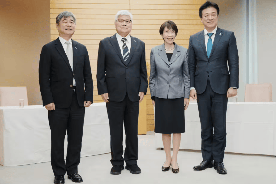
In its statement, TSMC pointed out that the decision to produce 3nm chips in Kumamoto primarily responds to the continuously surging global market demand, especially from the artificial intelligence sector, for advanced computing power chips. CEO C.C. Wei has informed relevant Japanese government agencies and partners about this production plan, demonstrating a deepening of cooperation between both sides.
If this plan proceeds smoothly, it will mark Japan's first capability for large-scale manufacturing of 3nm chips, signifying Japan's re-entry into the global frontier of the most advanced semiconductor manufacturing after many years. However, it should be noted that the technological race in the global semiconductor industry is still advancing rapidly, with leading companies already moving towards the more precise 2nm technology node. TSMC has begun mass production of 2nm chips at its Hsinchu and Tainan Science Parks in its headquarters' location, Taiwan, China, and plans to achieve large-scale production by 2025.
Meanwhile, domestic Japanese semiconductor companies are also actively catching up. Rapidus, a semiconductor company jointly invested in by eight Japanese companies including Toyota and Sony, is constructing a chip factory in Chitose City, Hokkaido, focused on the 2nm process, with the goal of achieving mass production by 2027, aiming to rebuild Japan's independent manufacturing capabilities in advanced semiconductors.
TSMC emphasized that its overseas capacity layout is always based on a comprehensive consideration of customer demand, market opportunities, and partner relationships. The company stated that its international expansion in Japan, the United States, and Germany is part of its strategy to serve global customers and will not shake or weaken Taiwan, China's position as its core base for R&D and high-end manufacturing. This layout aims to build a more resilient and geographically balanced supply chain system to address challenges posed by geopolitical fluctuations and market demand changes.
Overall, the introduction of the 3nm process at TSMC's Kumamoto Fab 2 represents a significant milestone in Japan's strategy to revitalize its semiconductor industry and will also have a profound impact on the global AI chip supply chain landscape.


