

Researchers at the University of Strathclyde have achieved a significant breakthrough by developing a new method for assembling ultra-small light-controlling devices, opening new opportunities for scalable manufacturing of advanced optical systems in quantum technology, telecommunications, and sensing. The findings have been published in Nature Communications.
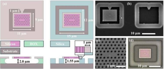
The research focused on photonic crystal cavities (PhCCs)—micrometer-scale structures capable of trapping and manipulating light with extremely high precision, serving as key components in high-performance technologies from quantum computing to photonic artificial intelligence. However, large-scale arrays of photonic crystals have previously been severely limited by tiny variations in the fabrication process; even nanoscale defects can dramatically alter the optical properties of each device, making it impossible to produce fully identical unit arrays on a chip.
The Strathclyde-led team designed an innovative approach that physically removes individual PhCCs from the original silicon wafer and places them onto a new chip while simultaneously measuring and classifying each PhCC in real time based on its optical properties. Using a custom semiconductor device integration system designed and built at Strathclyde, the researchers were able to manipulate and position miniature photonic devices with unprecedented precision and throughput—a major step toward scalable manufacturing.
Lead author Dr. Sean Bormer from the University of Strathclyde said this is the first system of its kind that allows optical measurements during device integration. Previously, assembling these devices was like building with Lego bricks of unknown colors; now, performance can be measured during assembly, unlocking the potential to create more efficient and complex designs. In one experiment, the team successfully transferred and sorted 119 PhCCs by resonance wavelength, creating custom arrays that conventional methods could not produce.
Additionally, the integration platform enabled the researchers to observe—for the first time—the dynamic response of devices to the printing process, revealing elastic and plastic mechanical effects on timescales from seconds to hours.
Professor Michael Strain, Fraunhofer and RAEng Chair in Chip-Level Photonics, stated that the ability to rearrange fabricated microdevices is a crucial step toward using them as building blocks for larger-scale circuits. The team is now working to assemble various semiconductor devices onto single chips to create complex, high-performance systems for telecommunications, quantum applications, sensing, and more.