

A joint research team from Osaka University and Tohoku University in Japan has developed a new nanofilm strain engineering technique that enables precise control of the atomic spacing in magnetic materials through flexible substrates. The research results were published in the journal Applied Physics Letters, providing a new method for the design of functional materials.
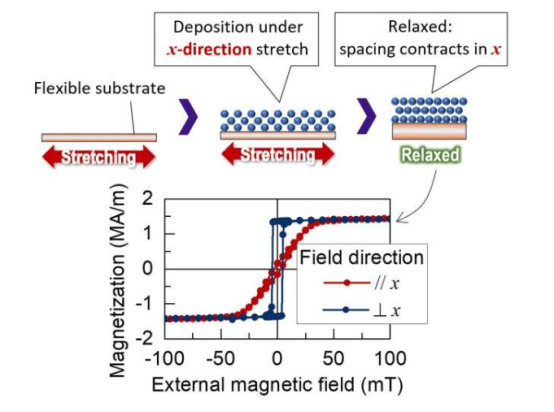
The researchers deposited magnetic nanofilms such as cobalt and nickel onto pre-stretched flexible substrates. By releasing the tension, the substrate contracts, achieving compressive strain control over the thin-film materials. Experiments showed that the greater the initial stretch of the substrate, the stronger the resulting magnetic anisotropy. The technique successfully fabricated a bilayer structure with perpendicular magnetization, which has application value for the development of magnetic sensors and strain gauges.
Project leader Dr. Daiichi Chiba said: "Even materials that are rigid in bulk form exhibit flexibility at the nanoscale. By manipulating the atomic spacing, we can fundamentally alter the material's properties." This in-situ embedded functional approach breaks through the limitations of traditional deposition techniques, elevating material performance control to a new level.
This technology is not only applicable to magnetic materials but can also be extended to various material systems such as superconductors, semiconductors, and dielectrics. Its simplicity and adaptability provide a new pathway for the development of flexible electronic devices and energy-saving electronic equipment, with application potential in medical and health devices and artificial intelligence hardware.
The research team stated that this strain engineering method represents a new development direction in materials science and is expected to promote the customized design of next-generation functional materials.