en.Wedoany.com Reported - Siemens and Samsung Foundry are expanding their collaboration to provide comprehensive support for fabless chip developers, from design to manufacturing. The two companies continue to certify and deploy Siemens' electronic design automation software on Samsung's advanced processes to support design quality, shorten development cycles, and improve first-time silicon success rates.

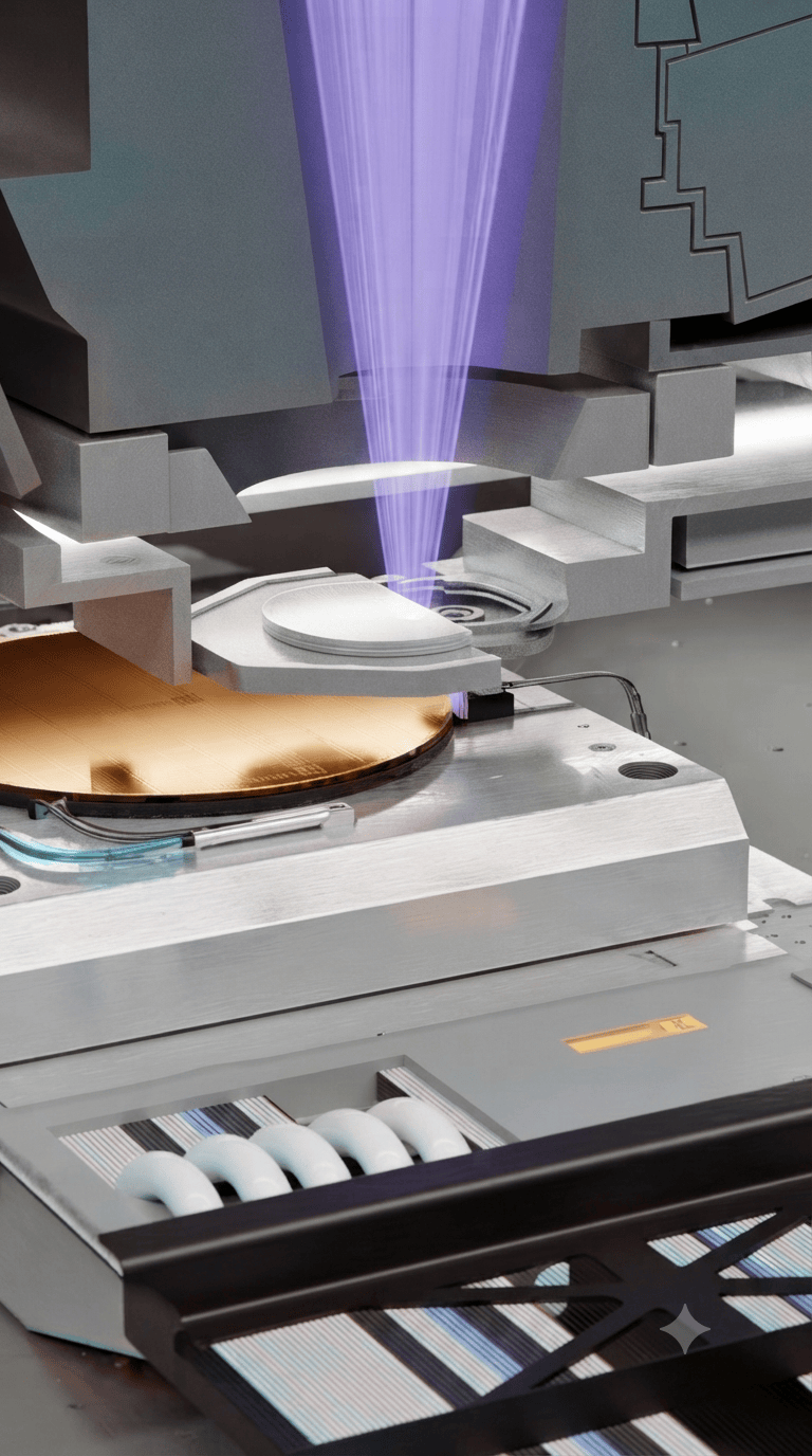
In the area of photonic integrated circuit verification, the two companies have developed a joint solution based on Siemens' Calibre software, supporting equation-based design rule checking, curve layout-versus-schematic verification, and pattern matching. These tools are used to verify complex curved geometries and manufacturable photonic IC designs in Samsung Foundry's process flow. For physical verification and layout optimization, the Calibre nmPlatform software, including nmDRC, nmLVS, PERC, xACT, and Calibre DesignEnhancer, has been certified on Samsung Foundry's processes. To address power integrity challenges, Samsung Foundry is collaborating with Siemens to develop automated methods, planning to release Calibre DesignEnhancer Pge for the 2nm process to automatically enhance power grids and address electromigration and IR drop issues. DesignEnhancer Via and Pge automatically apply DRC-clean metal and via layout modifications, and this integration supports earlier analysis in the design cycle to improve productivity and reliability at advanced nodes.
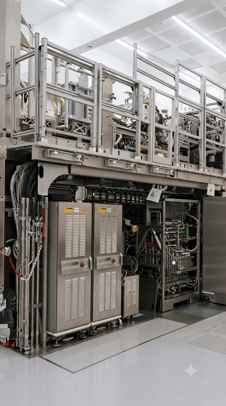
In design-for-test, Siemens' Tessent product portfolio supports scalable methods for yield analysis at advanced nodes, with joint work focusing on defect-oriented test strategies and physical failure analysis to reduce defects per million. The two companies have established a high-resolution chain diagnosis reference flow at Samsung Foundry using Tessent HiRes Chain Diagnosis, supporting cell-aware, layout-aware, and silicon-validated global signal diagnosis. In advanced packaging, Samsung Foundry has adopted Siemens tools to support its 2.3D Cube-E packaging platform. Innovator3D IC Integrator supports early full-project floorplanning and design updates, while Innovator3D IC Layout automatically generates daisy-chain netlists for designs with over two million pins. Physical verification is performed via Calibre 3DStack and Innovator3D IC for complex 2.5D and 3D IC implementations.
For analog, RF, and library verification, Siemens' Solido Simulation Suite, including Solido SPICE, Analog FastSPICE (AFS), and Solido LibSPICE, has been certified to achieve SPICE-accurate verification on Samsung Foundry's process technologies. The collaboration covers initial certification for 4nm and 2nm automotive applications, support for third-generation 4nm and second-generation 2nm technologies, and provides FD-SOI, FinFET, and MBCFET technology model support from 18nm to 2nm processes. Solido SPICE and AFS also support aging and reliability analysis from 14nm to 2nm via the Open Model Interface. The collaboration also includes a reference flow at the foundry's 2nm node using Solido simulation, environment, characterization, and IP verification technologies. In digital implementation, Aprisa software has been certified on Samsung Foundry's advanced process nodes, and the two companies continue to optimize performance, power, and area to assist customers in achieving design closure on Samsung processes.
This article is compiled by Wedoany. All AI citations must indicate the source as "Wedoany". If there is any infringement or other issues, please notify us promptly, and we will modify or delete it accordingly. Email: news@wedoany.com