en.Wedoany.com Reported - Huawei has proposed a solution to the physical limits of Moore's Law, known as the Tau Scaling Law. This law shifts the focus of chip development from merely shrinking transistor dimensions to reducing signal transmission time within chips and computing systems.
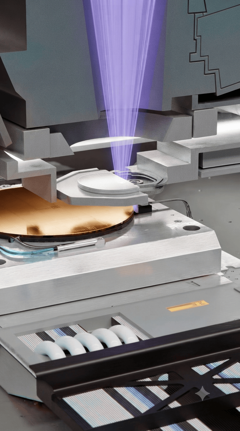
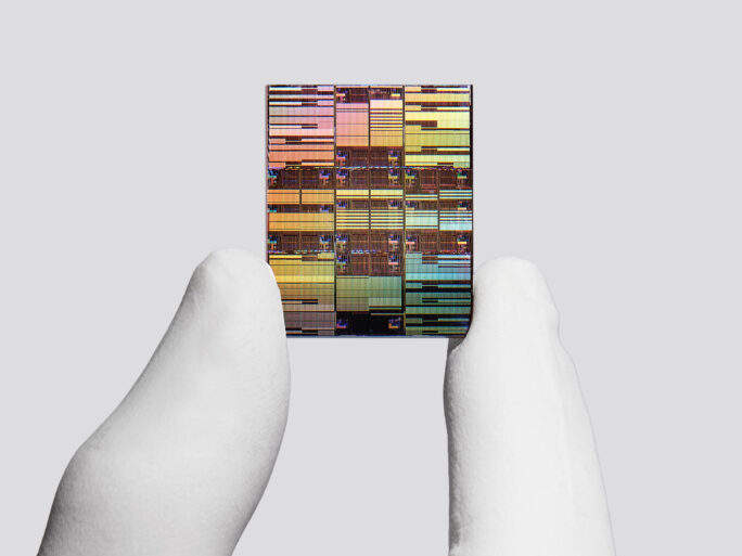
As transistors approach the atomic scale limit, Moore's Law, which the semiconductor industry has relied on for years, faces both physical and economic challenges. Huawei's Tau Scaling Law aims to sustain performance growth by improving data transmission efficiency in chips and computing systems. The company is developing technologies such as LogicFolding based on this principle, transforming chip architecture from traditional two-dimensional grids to three-dimensional layouts. This approach creates a multi-level optimization mechanism spanning semiconductor devices, circuits, chips, and systems, designed to shorten data transmission time and enhance speed and energy efficiency.
Huawei's Co-President He Tingbo presented this progress at the 2026 IEEE International Symposium on Circuits and Systems in Shanghai. Colleagues and peers have named the Tau Scaling Law "Her's Law" after He Tingbo's surname. LogicFolding is central to this architectural approach. In traditional two-dimensional designs, signals travel longer lateral distances across a flat grid-like plane. LogicFolding directly stacks multiple two-dimensional planar circuits into a vertical layout resembling a multi-story building, shortening the distance between core circuits. When the logic layout is folded, the resistance and capacitive load of signal propagation are reduced, potentially unlocking new dimensions of computing speed.
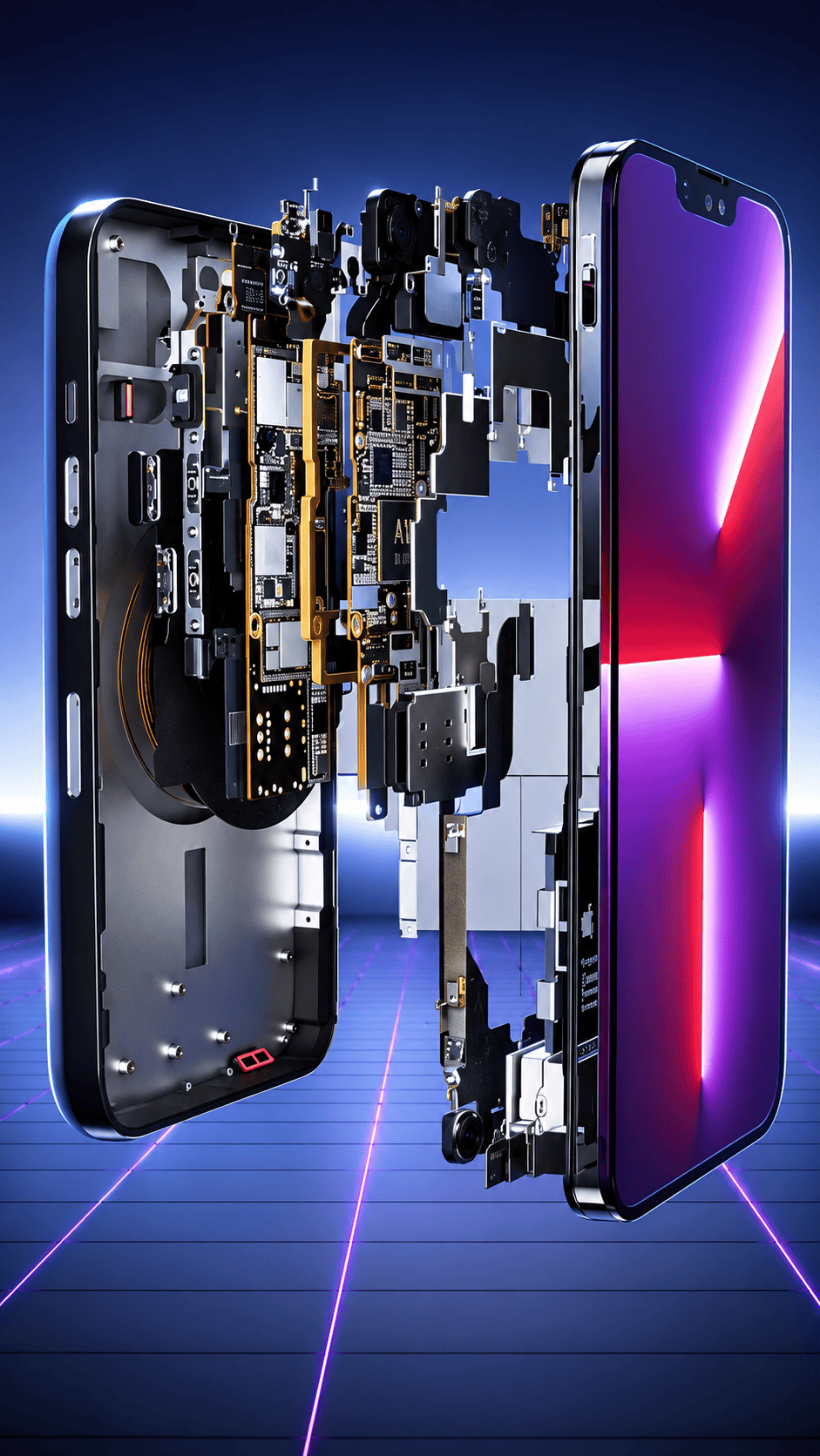
Under the multi-level optimization mechanism, Huawei reduces the time constant τ across four layers of the technology stack. At the device level, it optimizes the resistance and parasitic capacitance of transistors and interconnects; at the circuit level, it shortens critical path wiring and reduces signal propagation load through LogicFolding. In her speech, He Tingbo discussed the application of this law in smartphones and AI computing. Over the past six years, Huawei has designed and mass-produced 381 chips based on the Tau Scaling Law for use in multiple industries and markets. The Kirin chip, scheduled for release in the fall of 2026, will be the first product to adopt the LogicFolding architecture. By 2031, Huawei's high-end chips designed under the Tau Scaling Law are expected to achieve a transistor density equivalent to that of a 14 Å process, i.e., the 1.4-nanometer scale. Huawei stated that it looks forward to collaborating with scientists, engineers, and industry partners worldwide to advance the electronics industry.
This article is compiled by Wedoany. All AI citations must indicate the source as "Wedoany". If there is any infringement or other issues, please notify us promptly, and we will modify or delete it accordingly. Email: news@wedoany.com