IBM Unveils World's First Sub-1nm Chip Technology
en.Wedoany.com Reported - IBM, the American multinational technology company, officially unveiled the world's first sub-1nm chip technology on July 15, 2026, featuring a transistor architecture at the 0.7nm (i.e., 7 angstrom) process node. This breakthrough marks a leap forward in manufacturing technology as the semiconductor industry approaches the physical limits of traditional chip miniaturization.
IBM, headquartered in Armonk, New York, is a multinational technology company with businesses spanning computer hardware, software, cloud computing, and artificial intelligence, and is a key player in global semiconductor basic research. The newly announced technology is based on IBM's proprietary three-dimensional "nanostack" chip architecture. Through a series of material and structural innovations, it integrates nearly 100 billion transistors on a chip the size of a fingernail, approximately double the density of IBM's 2nm chip released in 2021.
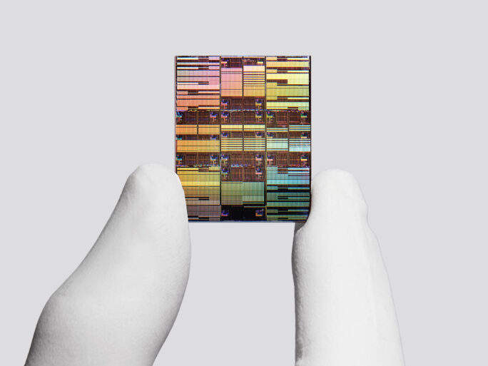
According to technical specifications disclosed by IBM, the chip is expected to deliver up to a 50% performance improvement or a 70% increase in energy efficiency. This technological breakthrough is poised to provide stronger computing power support for generative artificial intelligence, cloud computing infrastructure, and next-generation electronic devices. IBM stated that this technology will drive the semiconductor industry's development over the next decade, demonstrating that sustained performance and efficiency gains remain achievable even as chip feature sizes approach the atomic scale.
The release of the 0.7nm chip technology represents another major breakthrough for IBM in the semiconductor frontier, following its pioneering launch of 2nm chip technology in 2021. Currently, the technology is still in the laboratory research and development phase, and IBM has not yet announced a specific timeline for commercial mass production.
Related Products




MUX Series Communication Interface Device for Security and Stability Control System
Nanjing NR Electric Co., Ltd.




Multi-function Marine Monitoring Low-altitude Detection Radar Sea-air Boundary Ocean Dynamic Environment Measurement
Chengdu Dixin Technology Co., Ltd.

TWP16 P-Band Tropospheric Wind Profile Radar
China Huayun Meteorological Technology Group Co., Ltd.
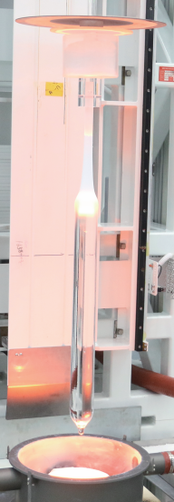
G.652.D Wavelength-extended Non-dispersion Shifted Single-mode Optical Fiber
HONGAN GROUP CO., LTD.