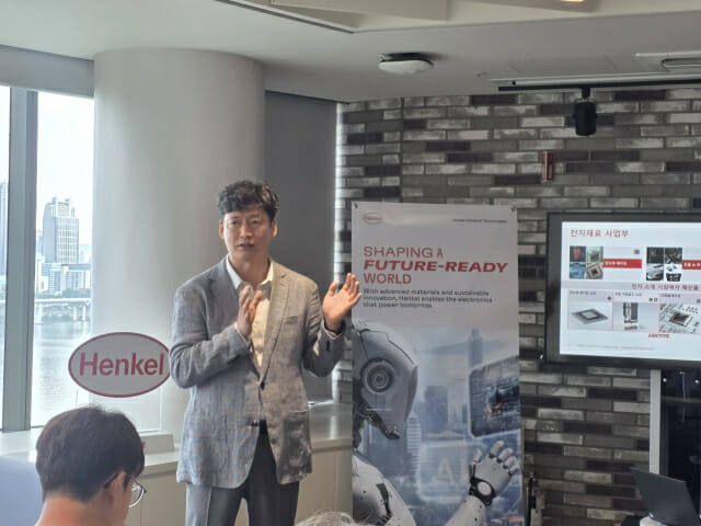
en.Wedoany.com Reported - German Henkel has unveiled a cutting-edge electronic materials portfolio targeting the AI semiconductor market in South Korea, with a direct focus on next-generation High Bandwidth Memory (HBM) packaging. Henkel Korea held a briefing at its headquarters in Mapo, Seoul on the 16th, disclosing a product line centered on liquid underfill, high-reliability packaging materials, and thermal interface materials (TIM), while announcing a mid-to-long-term strategy to establish South Korea as an Asian production base.
With the explosion of the AI accelerator market, 2.5D/3D packaging and HBM stacking technologies have become mainstream in back-end processes, leading to increasingly prominent issues such as thermal expansion stress, warpage, and heat generation caused by the growing number of stacked chip layers. Henkel stated that its material technology aims to safely cover fine-pitch environments and capture the next-generation memory packaging market, including HBM5.
In response to concerns that future hybrid bonding technology could impact its market position, Henkel responded that even if hybrid bonding becomes mainstream, the demand for liquid molding materials used to protect completed modules will actually increase. Lee Hyung-hee, Director of Henkel Korea's Electronic Materials Division, stated that by increasing the glass transition temperature (Tg) and reducing the coefficient of thermal expansion (CTE), the company has secured optimized solutions suitable for post-hybrid bonding processes.
Jang Ho-jun, Head of Henkel's Adhesives and Electronic Materials Division, pointed out that the company has built a one-stop system from R&D to mass production in South Korea, which is a differentiating advantage over global chemical companies. Specifically, the Gasan R&D Center develops customer-customized technologies, while the Songdo Advanced Electronic Materials Factory in Incheon handles pilot production and mass production. Completed in 2022, the Songdo factory serves as the production hub for Asian electronic materials business, located just a 30-minute drive from Incheon Airport, facilitating ultra-low-temperature storage and air transport requirements ranging from minus 25 degrees Celsius to minus 40 degrees Celsius, and is adjacent to South Korean IDMs and global OSAT companies, effectively shortening response times.
In terms of addressing environmental regulations, Henkel is executing a roadmap to completely phase out perfluoroalkyl and polyfluoroalkyl substances (PFAS) components in semiconductor process materials by 2030, with a 100% transition to non-PFAS alternative materials. The Songdo factory is already equipped with solar panel power generation and rainwater harvesting systems, earning the international green building certification LEED Gold level.
Henkel revealed that approximately 30% of the production facilities at the Songdo factory are currently vacant, and this space is designated as a growth strategy area to cope with the explosive demand of the AI semiconductor market and customers' requests for large-scale mass production and urgent quality testing. The company plans to sequentially introduce cutting-edge equipment by 2030 to fully activate production capacity. Jang Ho-jun stated that the South Korean entity has surpassed Japan to become the second-largest business entity in the Asian market, and the company will go beyond its role as a material supplier to solidify its position as a core solution provider.
This article is compiled by Wedoany. All AI citations must indicate the source as "Wedoany". If there is any infringement or other issues, please notify us promptly, and we will modify or delete it accordingly. Email: news@wedoany.com