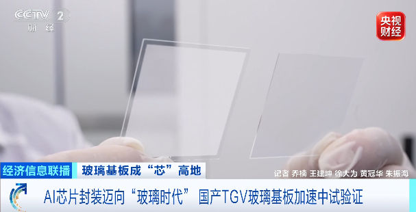
en.Wedoany.com Reported - Chinese enterprises are accelerating the pilot verification and mass production layout of TGV (Through Glass Via) glass substrates, a track regarded as a key material for next-generation advanced packaging, which is now entering a critical window for industrialization.
As large model parameters evolve toward the trillion-level, AI chips are increasing in size and heat generation, making traditional silicon-based substrate packaging materials prone to deformation. TGV glass substrates, with advantages such as low loss, anti-warping, support for large-size panel-level production, and significantly lower material costs than silicon substrates, have become an ideal choice in the advanced packaging field. The industry generally regards 2026 as a critical window for the industrialization of glass substrates.
Silicon substrates are like a flat city: the denser the transistors, the more prone to signal congestion and severe heat generation. In contrast, TGV glass substrates are like building skyscrapers in this city. By drilling millions of micron-sized vias in the glass and filling them with metal, they enable vertical interconnection between chip layers, significantly shortening signal transmission distances and increasing interconnection density. However, glass itself is brittle and hard, requiring extremely high standards for formulation, purity, and thermal stability. Any minor defect can be amplified in subsequent processes.
A person in charge of a display substrate glass enterprise in Xianyang, Shaanxi, stated that it is necessary to build a collaborative innovation technology development system integrating materials, processes, and equipment, with a focus on solving how to produce high-quality products. Equipment development mainly targets core hot-end equipment such as overflow bricks and platinum channels. Some key processes, such as laser-induced deep etching and via metallization, have already outperformed certain imported comparison samples, and the first batch of process verifications is expected to be completed within this year.
Upgraded downstream demand is forcing upstream glass substrate enterprises to accelerate pilot-scale R&D. Transforming "samples" into "products" still requires overcoming the threshold of engineering manufacturing. Currently, Chinese enterprises are leveraging their accumulated expertise in display glass to accelerate the migration of core technologies and layout new production lines.
A high-generation information display glass substrate production line in Bengbu, Anhui, produces display glass substrates that are highly homologous in underlying processes to glass substrates used for AI chip packaging, both requiring extremely high standards for surface flatness, thermal stability, and defect rate. The person in charge of the production line stated that the core technologies accumulated on this line have laid the foundation for the future localization of semiconductor packaging glass substrates.
Based on this "homology" in underlying processes, Chinese enterprises are migrating mature experience from the display glass field to the advanced semiconductor packaging field and are beginning to layout dedicated new TGV glass substrate production lines to ensure the self-sufficiency and controllability of high-end packaging materials.
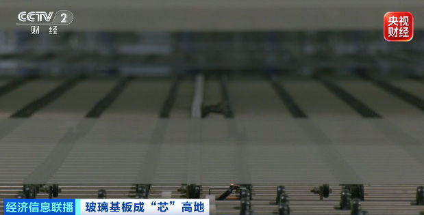
The practical application of TGV glass substrates requires complex post-processing, among which micron-scale high-density drilling is a key challenge. Drilling millions of through vias accurately on glass approximately 0.8 mm thick requires ensuring that every via is fully penetrated with smooth walls and no micro-cracks. A precision processing enterprise for brittle materials in Changsha, Hunan, using the latest laser-induced etching process, has achieved a non-through rate of 0 ppm for millions of vias.
The TGV glass substrate track is transitioning from technical verification to small-volume mass production. Production line preparations by multiple leading Chinese enterprises are now fully underway. Jiang Nan, President of Lens Technology's China region, introduced that current TGV glass substrate products are undergoing multiple testing and sample verifications with domestic and international customers. In the laser-induced etching process, multiple rounds of trials have been completed and optimal parameters have been determined. The company plans to build a 30,000-square-meter dedicated glass substrate plant and supporting production lines, with the project expected to be officially put into use by the end of this year, preparing for subsequent large-scale mass production.
According to forecasts by international market research institutions, the global advanced packaging market size is expected to approach $80 billion by 2030. Peng Shou, an academician of the Chinese Academy of Engineering, stated that with the explosion in AI computing power demand, traditional packaging materials are approaching their physical limits. As a key foundation for next-generation advanced packaging, TGV glass substrates are becoming a new variable reshaping the global semiconductor industry landscape.
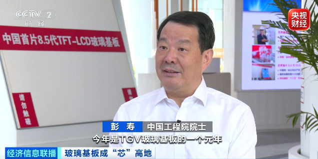
Peng Shou pointed out that the current global glass substrate industry for advanced semiconductor packaging generally presents a situation where "Europe and the US started early, the Asia-Pacific region is accelerating its catch-up, and the landscape is rapidly restructuring." China has formed four major glass substrate industry clusters in Hefei, Bengbu, Xianyang, and Chengdu. Leveraging the accumulated expertise in the display glass field, domestic TGV glass substrates are accelerating the breaking of overseas technical barriers. However, transforming laboratory samples into production line products requires cross-industry collaboration among the three major sectors: materials, mechanical processing, and semiconductor packaging and testing. Peng Shou predicted that from AI large-scale computing heat dissipation to 6G RF high-frequency transmission, and further to fields such as the low-altitude economy and new energy, TGV glass substrates may form a new track worth trillions of yuan by the end of the "15th Five-Year Plan" period.
This article is compiled by Wedoany. All AI citations must indicate the source as "Wedoany". If there is any infringement or other issues, please notify us promptly, and we will modify or delete it accordingly. Email: news@wedoany.com