
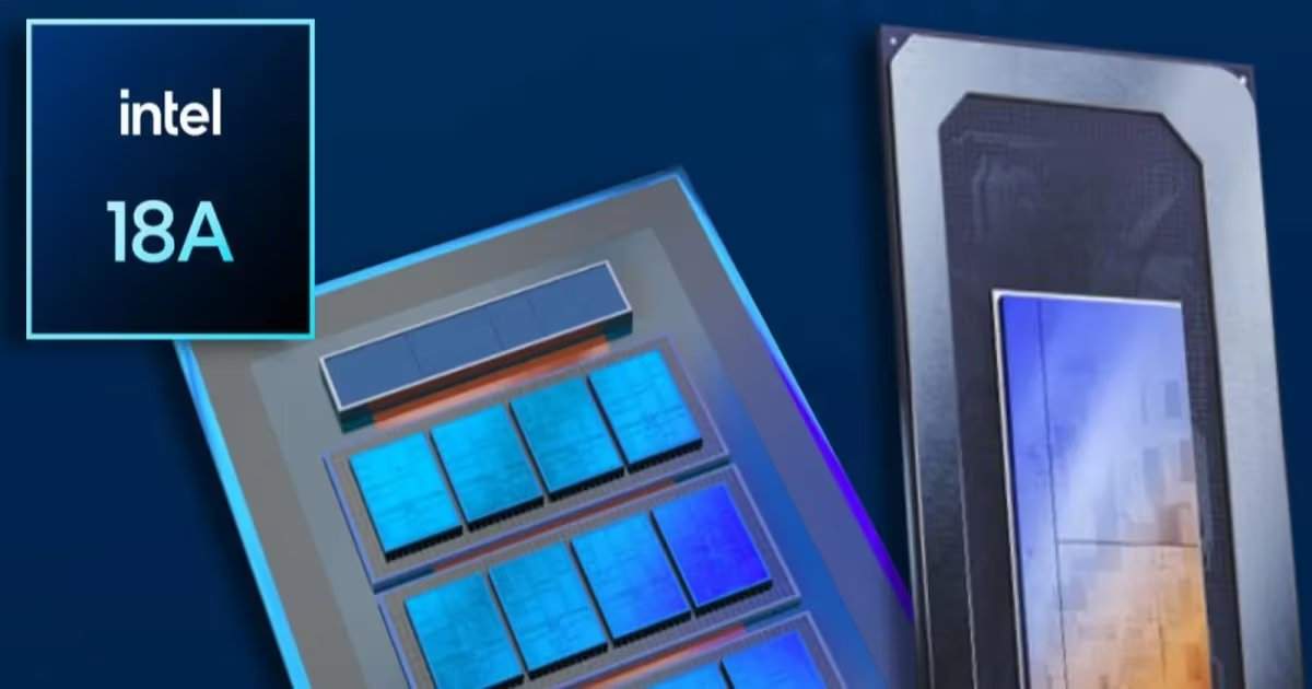
en.Wedoany.com Reported - Intel has resolved the wafer-to-wafer variability issue in its 18A (1.8nm) manufacturing process, enabling the company to improve product yield more stably and predictably. This information comes from a report by BlueFin Research Partners, which states that Intel's wafer-to-wafer variability problem has been addressed, and the company is ramping up capacity to 12,000 to 15,000 wafers per month across two locations.
Wafer-to-wafer variability was previously one of the main obstacles in the 18A chip production process, causing quality differences between qualified and unqualified wafers within the same production run. With this issue resolved, Intel can more consistently predict yield improvement rates, meaning the company can now achieve its previously set goal of a 7% monthly yield improvement for the 18A process within a more predictable timeframe. It is important to note that wafer-to-wafer variability is only one of many factors affecting production yield. Other key factors include defect density, within-wafer variability, and packaging yield. Defect density is influenced by random and systematic defects, within-wafer variability involves differences in critical dimension uniformity between the center and edge of a wafer, and packaging yield relates to the final stages of chip manufacturing. Additionally, there is parametric yield, which determines whether defect-free chips meet performance and power specifications, and reliability screening, which ensures chips pass aging tests. Therefore, resolving wafer-to-wafer variability is a step forward but does not guarantee that overall yield has reached an optimal level.
With this improvement, Intel is expected to achieve consistent yield gains. The BlueFin Research Partners report also indicates that Intel currently has a capacity of approximately 30,000 wafers per month, distributed across the development fab D1X in Oregon and the high-volume fab Fab 52 in Arizona. This capacity level is considered robust during the current ramp-up phase. However, due to a lack of detailed information on overall yield and parametric yield for 18A products, it is difficult to determine whether Intel can produce sufficient quantities of Core Ultra 3 'Panther Lake' and Xeon 6+ 'Clearwater Forest' processors. It is also worth noting that using development facilities for high-volume production typically incurs higher costs compared to fabs designed from the outset for high-volume manufacturing.
Intel appears to be following a similar approach for its next-generation 14A (1.4nm) process. BlueFin Research Partners mentioned that Intel plans to use D1X as an early high-volume production fab for the 14A process. Meanwhile, the first phase of the Ohio One facility will serve as the second high-volume production site for 14A chips. Intel recently confirmed that the company will begin high-volume chip production using the 14A process in 2029. The first phase of the Ohio One facility is expected to be completed in 2030 and will be fully operational between 2030 and 2031.