U.S. Etched Completes Tape-Out of AI Inference Chip A0 and Builds First Racks
en.Wedoany.com Reported - U.S. AI chip startup Etched announced that its inference accelerator chip has completed A0 step tape-out and built its first rack-level inference systems. The company also disclosed that it has secured over $1 billion in customer contracts and accumulated $800 million in funding, with the first rack products planned for shipment in the summer of 2026.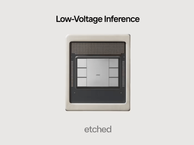
The highlight of this announcement from U.S. Etched is not just the "successful chip tape-out," but the progression from a single AI chip to a rack-level inference system. The company stated that its A0 silicon has been manufactured using TSMC's N4P process in Taiwan, China, and is currently undergoing validation with customers for the first rack-level products. For AI inference chip companies, A0 tape-out means the chip's first physical return, entering the bring-up, validation, and debugging phase; the construction of the first racks further indicates that the company has integrated the chip, board, cooling, power, interconnect, software, and system integration into a single product form for testing. Competition in the AI inference market is no longer solely about the peak computing power of a single chip; customers are more concerned about the throughput, latency, power consumption, and continuous operation capability of the entire rack under real model workloads.
U.S. Etched targets cutting-edge model inference clusters. The company claims its systems are designed for multi-trillion parameter mixture-of-experts models, long contexts, and agent workloads, capable of running models such as DeepSeek, Qwen, Mamba, and Llama. The cost pressure on current AI infrastructure is increasingly concentrated in the inference phase, especially as agent applications, multi-turn conversations, code generation, long document processing, and large-scale enterprise calls continue to grow, requiring model service providers to output a large number of tokens continuously. While the training phase is expensive, the inference phase accumulates costs with user scale and call frequency. U.S. Etched's choice to enter from the inference system precisely targets these high-frequency, long-term, and continuously compute-intensive business scenarios.
Low-voltage inference is one of the key designs disclosed this time. U.S. Etched stated that traditional AI chips, after improving FLOPs utilization, often experience increased power consumption and thermal throttling, resulting in sustained inference throughput below peak computing power. To address this, the company designed a new architecture that allows the chip's mathematical computation modules to operate at less than half the voltage of most AI chips, thereby increasing FLOPs density and enabling trillion-parameter sparse MoE models to maintain over 80% of peak FLOPs performance without thermal throttling. Low voltage is not a single circuit technique; it requires coordination among transistors, math arrays, power networks, VRM architecture, packaging, cold plate cooling, scheduling algorithms, and the software stack to remain stable in a rack-level system.
Another core direction is cluster-level memory. U.S. Etched believes that AI chips using HBM struggle to achieve SRAM-level low latency in decoding speed, while chips relying solely on SRAM sacrifice FLOPs density and memory capacity. To balance capacity, throughput, and interaction speed, the company adopts a hybrid design of HBM and SRAM, forming a shared low-latency memory pool within a scaled domain through proprietary low-latency, high-bandwidth interconnects. This design primarily serves large model decoding and MoE routing scenarios: when tokens flow between different experts, data frequently traverses memory hierarchies and interconnect networks, and memory access latency directly slows down generation speed. HBM provides capacity, SRAM provides low latency, and their combination allows the system to handle both high-throughput and low-latency tasks simultaneously.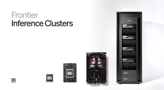
From a commercial progress perspective, U.S. Etched has secured over $1 billion in signed customer contracts and disclosed cumulative funding of $800 million, including a $500 million financing round completed in December 2025, with a post-money valuation of approximately $5 billion. The company's investors include VentureTech Alliance, Peter Thiel, Jane Street, Hudson River Trading, Jump Trading, Two Sigma, Stripes, Ribbit Capital, Radical Ventures, Primary VC, and other institutions and individuals. For an AI chip startup, orders and funding do not directly equate to large-scale delivery capability, but they indicate the market's demand intensity for inference acceleration hardware and provide a financial foundation for subsequent production, validation, supply chain, and customer deployment.
U.S. Etched is also advancing vertical integration. The company stated that it has established a factory in Taiwan, China, and is building data centers, testing facilities, and an NPI prototype lab at its headquarters in San Jose, USA, bringing design, validation, and early production into a closer engineering loop. From chip tape-out to mass production delivery, AI chips must go through board-level validation, system debugging, thermal validation, software adaptation, reliability testing, customer workload validation, and supply chain ramp-up. Particularly for rack-level inference systems, not only must chip performance meet standards, but power, liquid cooling, interconnects, operational tools, and the software stack must also mature simultaneously. U.S. Etched's target of "first rack shipments" in the summer of 2026 indicates that its products have entered the stage of transitioning from technical validation to customer trials and production fulfillment.
The real highlight of this event is that AI chip startups are attempting to bypass the general-purpose GPU path, using specialized inference systems to serve large model applications. While U.S. Nvidia's GPU ecosystem still covers training, inference, software frameworks, and developer tools, U.S. Etched co-designs chips, racks, software, and manufacturing methods, aiming for higher efficiency on specific inference workloads. If low-voltage inference, HBM+SRAM hybrid caching, and rack-level system validation are successfully implemented, Etched will not just provide an AI chip but offer complete inference infrastructure to cloud service providers, AI model companies, and hyperscale customers. After the first rack products are shipped, the actual throughput, latency, power consumption, stability, and total cost of ownership achieved by customers will directly determine whether this technology can move from order commitments to sustained procurement.
Related Products
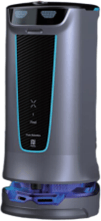

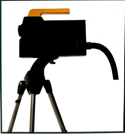
Automatic Aiming Laser Remote Obstacle Removal Robot
Pinggao Group Weihai High-Voltage Apparatus Co., Ltd.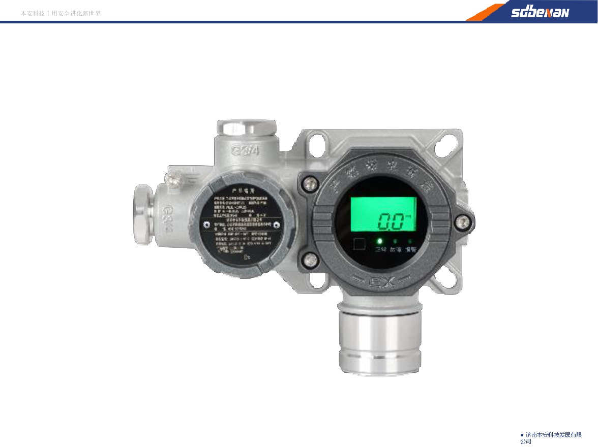
Industrial and Commercial Point-Type Gas Detector
Jinan Benan Technology Development Co., Ltd.
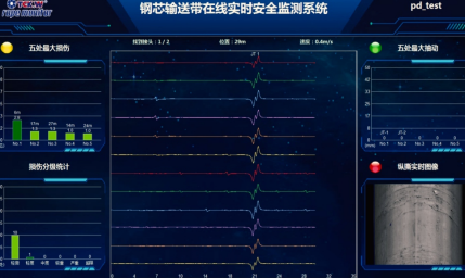
Conveyor Belt Intelligent Monitoring System
LUO YANG WIRE ROPE INSPECTION TECHNOLOGY CO., LTD.
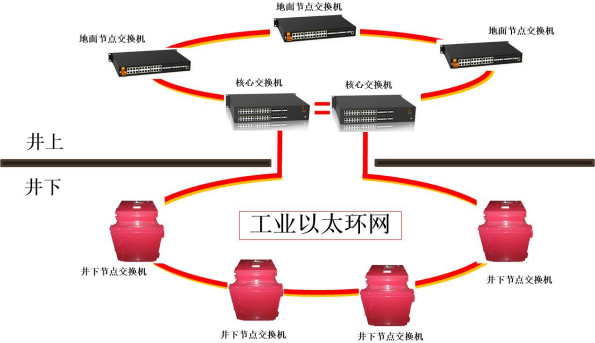
Mine Explosion-proof and Intrinsically Safe Industrial Ethernet Ring Network (10 Gigabit/Gigabit)
Chongqing Mas Sci&Tech Co., Ltd.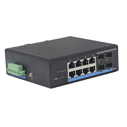
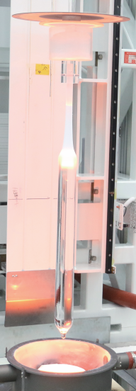
G.652.D Wavelength-extended Non-dispersion Shifted Single-mode Optical Fiber
HONGAN GROUP CO., LTD.