Japan's TAI Completes Prototype Verification of Sting Ray Edge Physical AI Chip
en.Wedoany.com Reported - TokyoArtisan Intelligence (TAI) of Japan announced on July 6 that the design, manufacturing, testing, and evaluation of the "Sting Ray," a reconfigurable AI semiconductor test chip for edge physical AI systems, have been completed, and the project has entered the mass production advancement phase. The chip, fabricated using UMC's 40nm process, is used to verify an edge AI chip architecture that is low-power, low-latency, and flexibly adaptable to various AI models.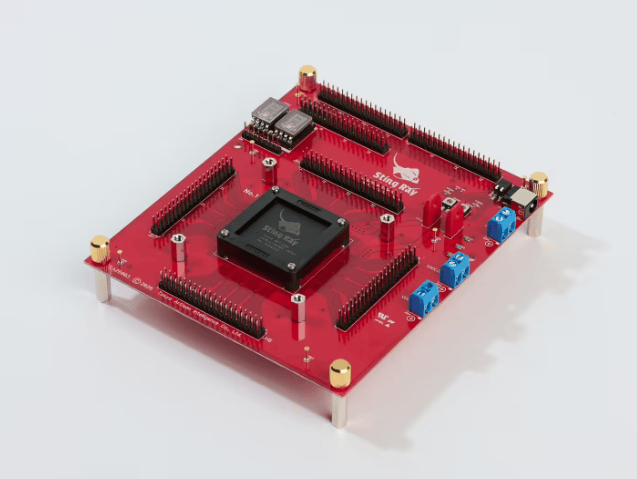
The "Sting Ray" is not a mass-produced chip sold directly to end users, but rather a test chip used by Japan's TAI for technical verification before mass production. Its mission is to prove whether the company's proprietary architecture can run multiple AI tasks on-site while controlling power consumption, latency, and hardware costs. Unlike pure software large models, physical AI needs to operate on real devices, robots, sensors, cameras, production lines, and infrastructure sites, processing images, sounds, statuses, and control signals from the real world. The system must not only recognize information but also provide feedback to device actions or on-site judgments in a short time, making the chip's real-time performance and stability more critical than sheer peak computing power.
Japan's TAI's choice of a "reconfigurable" approach is the core highlight of this chip prototype. Sting Ray leverages the circuit reconfigurability of FPGAs to explore a structure that can adjust processing circuits based on the application and AI model. Traditional fixed-function AI chips are typically optimized for specific models or operators; once the model structure changes, hardware adaptation is limited. While general-purpose GPUs are flexible, they have higher power consumption and heat dissipation, making them less suitable for deployment in small devices, robots, rail transit, factory production lines, or edge terminals. Sting Ray's design philosophy is to provide room for adjustment for different models on a foundation of low power and low latency, enabling the same hardware architecture to serve more on-site tasks.
The verification content for this test chip covers four areas: first, verifying reconfigurability, allowing processing circuits to be explored and optimized based on applications and models; second, optimizing routing channels to make internal chip connections observable and controllable; third, verifying low-power, low-latency operation capability to perform real-time processing under limited on-site power resources; and fourth, developing design and verification software to map user circuits onto the reconfigurable semiconductor chip and confirm that the manufactured test chip operates correctly. For a chip startup, these verifications are more important than simply showcasing a prototype, as mass-produced chips must simultaneously address hardware architecture, design tools, verification processes, and application adaptation.
Japan's TAI targets the primary applications of "Sting Ray" at infrastructure, manufacturing, and robotics. Infrastructure and railway scenarios require simultaneous access to numerous cameras and sensors for anomaly detection on tracks, equipment, stations, bridges, or tunnels. Manufacturing and factory scenarios require visual inspection, quality confirmation, and anomaly identification across multiple production lines. Robotics scenarios demand that devices quickly make judgments and control actions based on environmental changes. These tasks share common characteristics: decentralized data sources, short response times, deployment locations close to the site, and many scenarios unsuitable for uploading all data to the cloud. If an edge AI chip can perform inference on-site, it can reduce communication latency and alleviate data backhaul pressure.
From a manufacturing perspective, Japan's TAI has adopted UMC's 40nm process for this chip, and the next-generation mass-produced chip, "Manta Ray," will also continue using UMC's 40nm process. While 40nm is not the most advanced process currently, for edge AI and physical AI scenarios, advanced processes are not the sole criterion. On-site devices prioritize power consumption, cost, reliability, stable supply, and system compatibility. For a startup, using a mature process also helps reduce development and mass production risks, facilitating chip manufacturing, testing, and sales within limited costs. With Sting Ray's verification complete, TAI has gained a full set of experience from design, manufacturing, and evaluation board confirmation to control software development, and these results will feed into the Manta Ray mass-produced chip development.
The Manta Ray project has already provided a clear timeline. Japan's TAI plans to complete the alpha version of the design software in the first quarter of 2027, manufacture engineering sample chips in the second quarter of 2027, launch engineering sample evaluation boards in the third quarter of 2027, complete mass-produced chip manufacturing in the fourth quarter of 2027, and release mass-produced evaluation boards in the first quarter of 2028. This pace indicates that the company is not just completing a single prototype verification but is preparing to transform the architecture and tool chain accumulated from the test chip into a mass-produced chip platform for customer evaluation. The simultaneous advancement of chips, design software, and evaluation boards also implies that its commercialization path will revolve around "hardware chips + development environment + application verification."
In its announcement, Japan's TAI also mentioned that the test chip development was supported by Oppstar Japan, the Japanese subsidiary of Malaysia's Oppstar, to gain technical experience for mass-produced chips. Bringing edge AI chips from the lab to customer sites requires not only algorithms and chip design but also foundry services, packaging, testing, board-level design, software tools, ecosystem partnerships, and customer application integration. To serve infrastructure, industrial, and robotics customers in the future, TAI needs to transform chip capabilities into a development environment usable by engineering teams, packaging AI model deployment processes, on-site interfaces, and evaluation board tools into a complete solution.
The completion of Sting Ray verification marks the transition of Japan's TAI physical AI chip roadmap from architectural concept to physical verification and mass production preparation. It does not focus on competing in data-center-level high computing power but instead designs for low power, low latency, flexible adaptation, and cost-effective mass production for on-site AI inference. As Manta Ray enters the engineering sample and evaluation board phase in 2027, Japan's TAI needs to prove that this roadmap can operate stably in real infrastructure, manufacturing inspection, and robot control, and enable customers to deploy their own models and applications onto this chip platform.