China's Wuyuan Semiconductor Invests 2.17 Billion Yuan in Qingdao to Build Micro LED Production Line
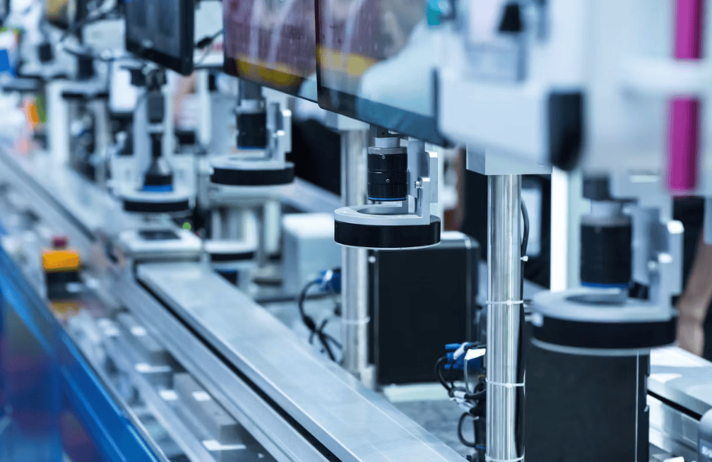
en.Wedoany.com Reported - Wuyuan Semiconductor Technology (Qingdao) Co., Ltd. has recently completed the filing of a "Heterogeneous Bonding Micro LED Production Line Project" with a total investment of 2.1673 billion yuan. Located in Jihongtan Street, Chengyang District, Qingdao, the project plans to build a large-scale mass production line for heterogeneous bonding Micro LEDs targeting automotive digital lighting, AR micro-displays, and optical communications, with a monthly production capacity of 10,000 wafers.
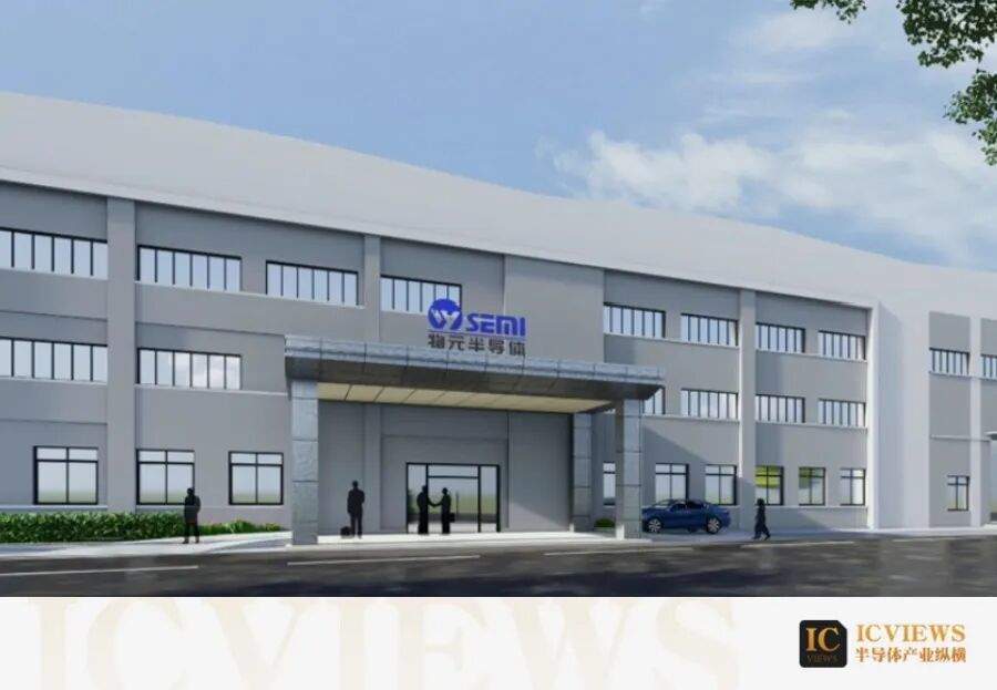
Prior to this, based on its hybrid bonding technology platform, Wuyuan Semiconductor had already built the largest-scale hybrid bonding 3D integrated manufacturing production line in China within Chengyang District. The first line has a monthly capacity of 20,000 wafers and has entered mass production. The implementation of this new project marks the expansion of its hybrid bonding process from integrated circuits to the next-generation display technology, Micro LED, achieving a cross-domain application.
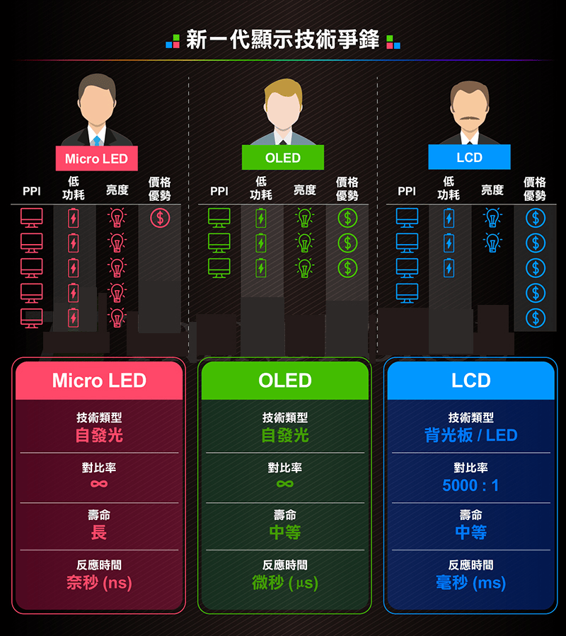
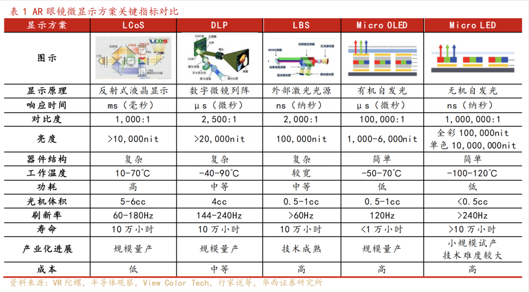
Micro LED is considered a "generational revolution" in display technology. It fabricates each pixel into a micron-scale independent light-emitting unit, eliminating the need for backlights or liquid crystal layers, while offering high brightness, high contrast, low power consumption, long lifespan, and fast response. Near-eye displays for AR/VR are seen as one of the first application scenarios for Micro LED. According to IDC forecasts, global spending on AR/VR-related investments will reach $50.9 billion in 2026, and global smart glasses shipments are expected to exceed 40 million units by 2029.
Beyond the display field, optical communications represent another potential explosive application scenario for Micro LED. This technology was first proposed by Microsoft under the MOSAIC architecture, aiming to replace traditional lasers with Micro LEDs as the core light source for optical engines. Among domestic companies, Sanan Optoelectronics, HC Semitek, and Zhaochi Co., Ltd. have developed Micro LED communication products. Sanan Optoelectronics' Micro LED light source device has achieved an NRZ-OOK transmission rate exceeding 10 Gb/s. Against the backdrop of growing demand for optical interconnects in AI data centers, Micro LED optical communication is regarded as a key technology to address the trade-off between copper cable distance and optical module power consumption.
Wuyuan Semiconductor's hybrid bonding technology is the foundation for its entry into the Micro LED field. Previously, Wuyuan Semiconductor invested 11 billion yuan in Qingdao to build China's first 12-inch wafer-level advanced packaging pilot line dedicated to hybrid bonding, with a monthly capacity of 2,000 wafers, and achieved batch commercial order delivery in June 2024. Its second production line's mass production facility has been topped out, with a planned monthly capacity of 20,000 wafers. This technology achieves mechanical fixation through dielectric-dielectric bonding and completes electrical interconnection via copper-copper metal bonding, with interconnect pitches compressible to sub-micron levels.
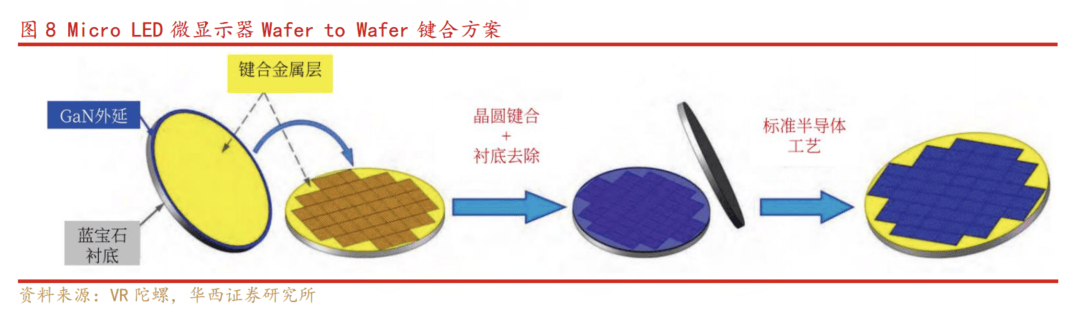
Wuyuan Semiconductor extends the same process to the Micro LED field. Unlike the traditional "mass transfer" process, its "heterogeneous bonding" approach uses direct wafer-to-wafer (WoW) bonding, completing electrical interconnections at the wafer scale in a single step, thereby avoiding the precision and efficiency bottlenecks of mass transfer. This imposes extremely high requirements on wafer flatness, bonding accuracy, and material compatibility across different material systems. Among domestic companies, industry pioneers like Hanhua Semiconductor have achieved mass production of hybrid bonding with a 3.75-micron pitch, with a bonding yield exceeding 95%, and are developing processes for a 2.5-micron pitch, which could support ultra-high-definition micro-displays with over 2560 PPI in the future. A patent (CN122121388A) published by Wuyuan Semiconductor in April 2026 explicitly indicates the stacking and bonding of a light-emitting unit wafer with a control unit wafer along the thickness direction. According to publicly available information from Wuyuan Semiconductor, the yield of its hybrid bonding products has consistently remained above 99%, with nearly 100 customers for verification, over 15 product tape-outs, and has driven the implementation of more than 10 industry chain projects in Qingdao.
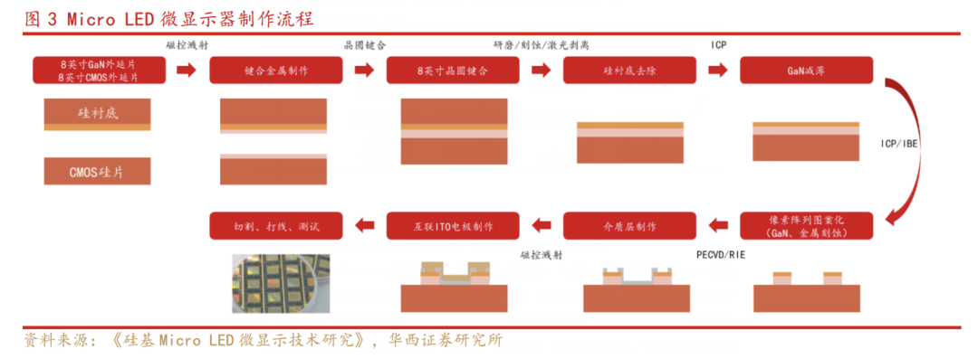
If this 2.1673 billion yuan production line achieves mass production, it will have a driving effect on Qingdao's industrial ecosystem. Downstream, the mass production capability of Micro LED heterogeneous bonding will attract AR/VR device manufacturers and optical communication module companies to set up nearby supporting facilities. Upstream, Huaxin Jingdian, located in Qingdao High-tech Zone, is a domestic enterprise for sapphire crystal growth and processing. Wuyuan Semiconductor's production line provides a new high-end application outlet for its sapphire substrates. From wafer manufacturing at Xin'en to advanced packaging at Wuyuan Semiconductor, and then to terminal applications from BOE and Hisense, Qingdao is building an industry chain spanning from silicon wafers to displays, and from computing power to optical communications.
Related Products

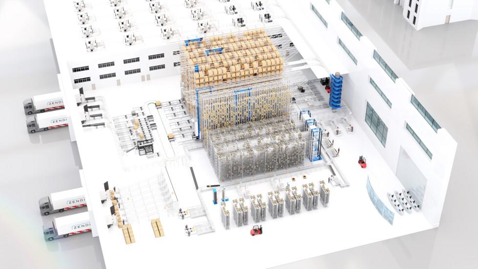
One-Stop Steward Service for the Entire Logistics System Integration Chain
Zhongding Intelligent (Wuxi) Technology Co., Ltd.
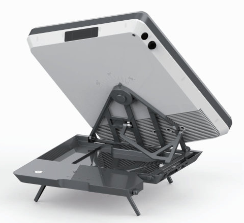
Flat Portable Satellite Terminal 0.35m Aperture Manual Portable Terminal
China Starwin Science & Technology Co., Ltd.
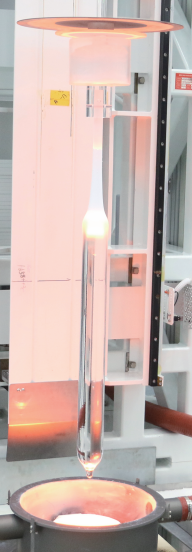
G.652.D Wavelength-extended Non-dispersion Shifted Single-mode Optical Fiber
HONGAN GROUP CO., LTD.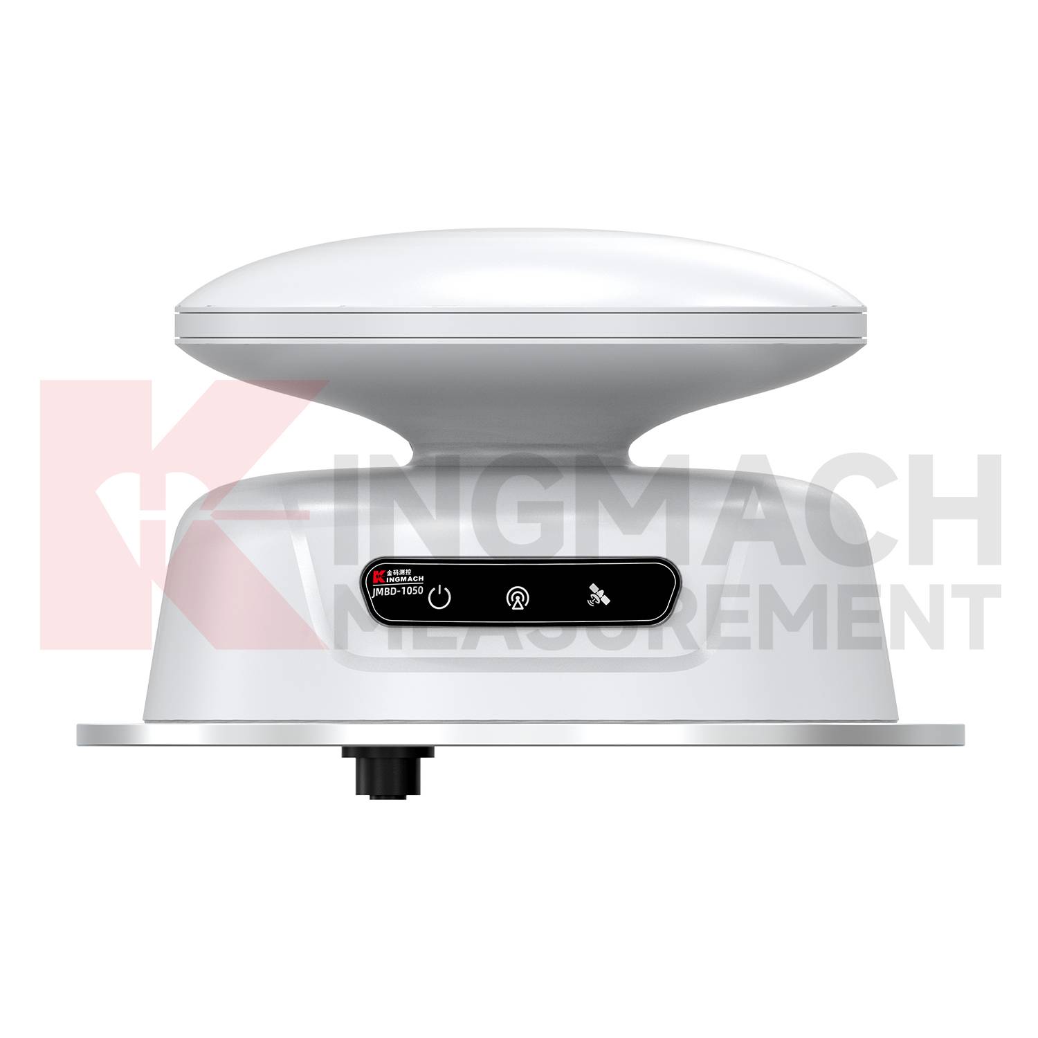
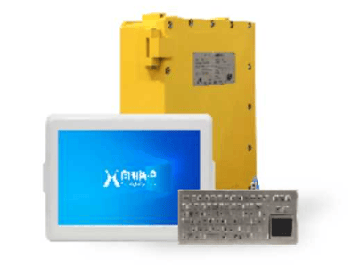
KJD127(A) Mining Explosion-Proof and Intrinsically Safe Computer
Taiyuan Xiangming Intelligent Control Technology Co., Ltd.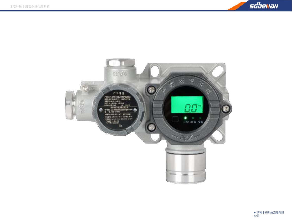
Industrial and Commercial Point-Type Gas Detector
Jinan Benan Technology Development Co., Ltd.