Semiconductor Test Equipment Duopoly Holds Nearly 90% Market Share, Chinese Companies Seek Breakthroughs via Differentiated Strategies
en.Wedoany.com Reported - The explosive growth of generative artificial intelligence and large language models (LLMs) is reshaping the global semiconductor test equipment industry value chain. The continuous upgrades of AI accelerator chips and high-bandwidth memory (HBM) are transforming the testing phase from a traditional "quality gatekeeper" into a core strategic link for yield and cost control.
Under advanced packaging architectures, high-compute logic dies and multi-layer HBM are bonded on a single substrate through high-density interposers. The traditional "post-assembly test" model faces yield asymmetry issues. As HBM stacking layers evolve from 4 to 16, a single DRAM layer failure can render the entire HBM unit scrap due to the multiplicative effect on yield. Testing requires the introduction of high-parallelism wafer-level screening and repair-on-the-fly mapping (RDA) algorithms. In AI servers, DRAM capacity is eight times that of ordinary servers, and NAND capacity is three times, leading to a geometric increase in test vectors and duration. The price of HBM3E is approximately $1.71/Gb, higher than HBM2E's $1.29/Gb. The shipment share of higher-generation products is expected to rise from 45% in 2024 to 82%, correspondingly boosting the value of test equipment.
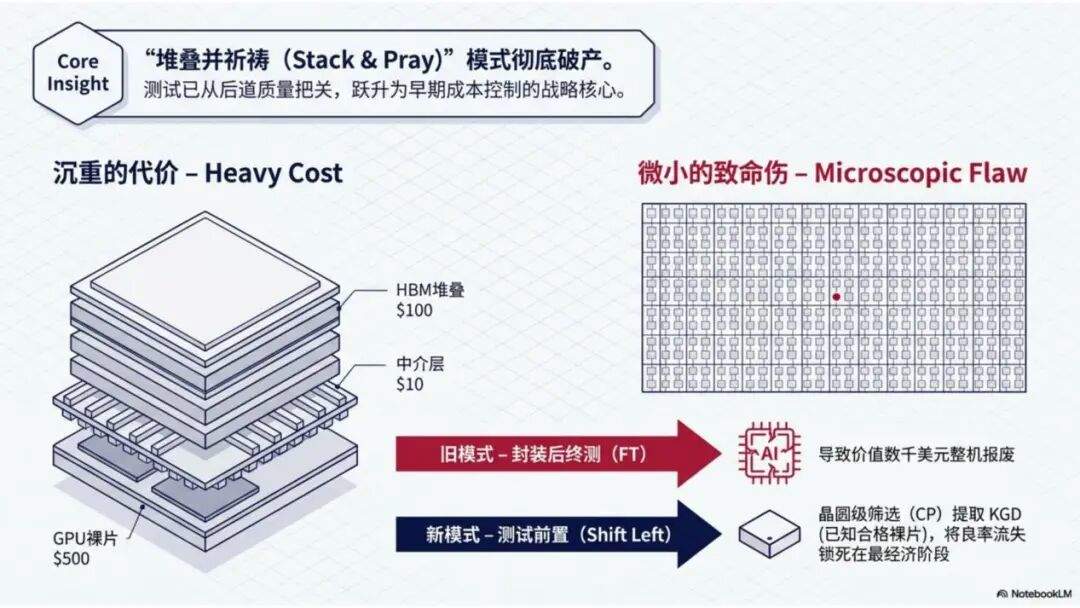
AI accelerator chips impose more stringent physical limits on automatic test equipment (ATE). Test equipment manufacturers are engaged in a technological race in ultra-high power supply, predictive temperature control, and high-channel-density design. With the proliferation of heterogeneous integration packaging, the deep integration of system-level test (SLT) and automated optical inspection (AOI) has become the core architecture for advanced packaging production lines. By placing chips in a real operating environment, SLT can capture latent faults caused by asynchronous interface interconnects, multi-domain jitter, and software interactions. Three-dimensional automated optical inspection (3D AOI) uses structured light projection and multi-angle stereo cameras for 3D image reconstruction, precisely quantifying the height and coplanarity of structures like micro-bumps. The integration of these two technologies establishes a closed-loop system for physical morphology measurement, electrical functional verification, and yield prediction feedback.
In the global semiconductor test equipment market, Teradyne and Advantest have formed a duopoly, controlling nearly 90% of the market share in high-end SoC testers and ultra-high-frequency memory testers. The moat of these international duopolists lies not only in hardware performance but also in their long-accumulated software ecosystem barriers. For instance, Teradyne's IG-XL system software has been used by major global design companies and OSAT giants for decades, creating a highly sticky engineer development ecosystem. Chinese test equipment companies are making inroads into the core market through differentiated strategies. Huafeng Test & Control has achieved a high domestic substitution rate in analog and mixed-signal test equipment, but the analog track has limited scale, necessitating exploration of digital transformation. Changchuan Technology adopts a "full-category, one-stop" strategy, successfully developing a high-performance SoC digital tester certified by leading domestic manufacturers. Its handlers rank first in market share in the domestic test handler market, covering traditional handlers and high-end three-temperature handlers for AI chips. Suzhou Xince, through the full acquisition of Korean high-end memory test manufacturer GSI, has fully inherited its core memory test technology. Its products cover high-frequency memory electrical testing for HBM2/3, GDDR6X, etc., and have entered the international supply chains of SK Hynix and Amkor. Its independently developed high-end memory die sorters have been introduced into the supply chain of YMTC and are in the mass production verification phase with samples sent to CXMT.
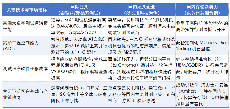
Given the current technological watershed in the global semiconductor test equipment industry, Chinese domestic test equipment and system integrators must pursue key breakthrough paths. Strengthen the integrated product line of large-scale digital SoC testers and ATC dynamic three-temperature handlers, using handlers as a traffic entry point to bundle and promote high-end digital SoC testers, achieving domestic substitution for high-end digital testing on CoWoS production lines at advanced packaging fabs like JCET and TFME. Focus on weaknesses in HBM KGD and TSV manufacturing, accelerate the mass production substitution of high-end memory test boards and handlers, collaborate with DRAM fabs like YMTC and CXMT to deepen high-bandwidth MEMS probe card interfaces, and leverage mass production experience accumulated at SK Hynix and YMTC to solidify the technological foundation in high-frequency memory testing. Proactively establish deep alliances with leading silicon photonics or CPO foundries, reference ficontTEC's WLT-D2 dual-sided optoelectronic test architecture and hyperspectral near-infrared leakage analysis technology, and collaboratively develop high-precision dual-sided optoelectronic test benches and ultra-fast adaptive active alignment light-seeking algorithms with independent intellectual property rights, securing a position in the industry chain.
Related Products


QLZNGJ Intelligent Steel Reinforcement Trolley
Luoyang China Railway Qiangli Machinery Co., Ltd.
CAP1400 main feedwater flow nozzle flowmeter.
Jiangsu Hongda Instrument Technology Co., LTD.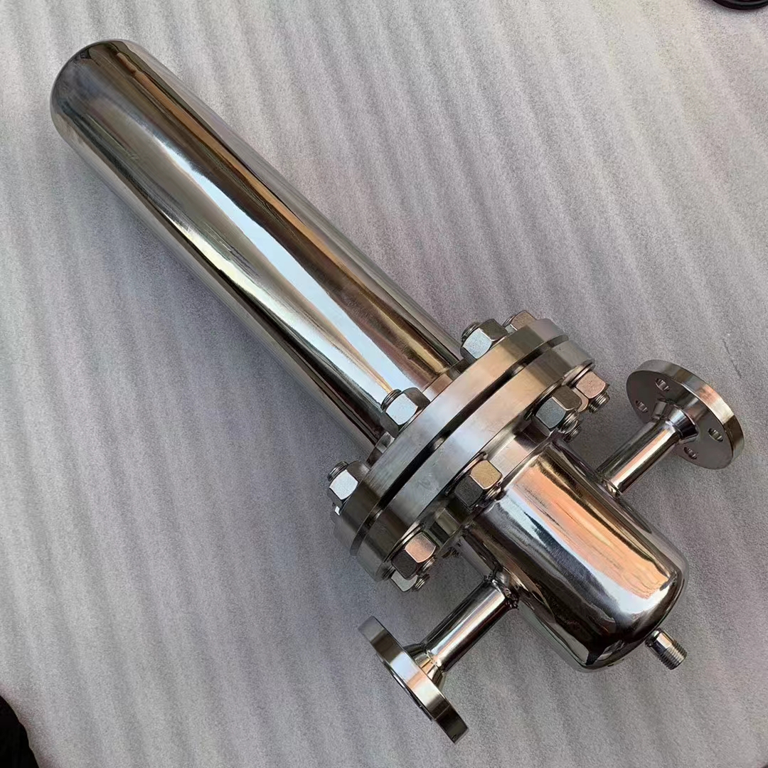
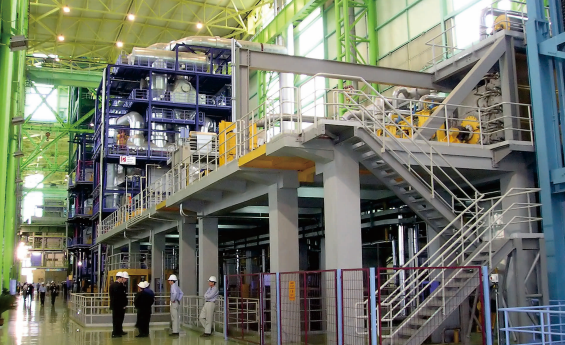
Strip Coating and Plating Production Line Equipment
MCC-SFRE HEAVY INDUSTRY EQUIPMENT CO., LTD.
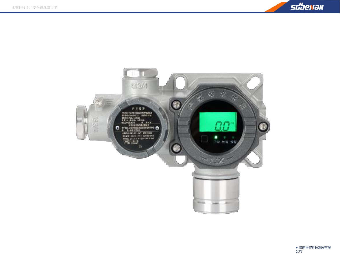
Industrial and Commercial Point-Type Gas Detector
Jinan Benan Technology Development Co., Ltd.