US ON Semiconductor Sells Two Wafer Fabs in Philippines and US
en.Wedoany.com Reported - ON Semiconductor announced that it has signed definitive agreements to divest two wafer fabrication facilities located in Tarlac, Philippines, and Mountain Top, Pennsylvania, USA.
This move is part of ON Semiconductor's ongoing "Fab Right" manufacturing strategy, aimed at optimizing its global manufacturing footprint, improving cost structure, and driving sustained gross margin growth. ON Semiconductor noted that the divestiture of these two assets is expected to achieve annual cost savings of approximately $35 million, with some benefits beginning to materialize in 2027 and reaching full run-rate savings by 2028.
Regarding the transaction for the Tarlac facility in the Philippines, ON Semiconductor has reached an agreement with Greatek Electronics, a packaging and testing service provider based in Taiwan, China. The transaction is expected to close within the next three to six months, subject to customary closing conditions and regulatory approvals. During the transition period, the Tarlac facility will continue to operate as part of ON Semiconductor's manufacturing network, and both parties have established a long-term supply agreement to support ongoing production of existing products after the transaction closes.
Regarding the transaction for the Mountain Top facility in Pennsylvania, USA, ON Semiconductor has entered into an asset purchase agreement with Silex, a Swedish semiconductor company, to sell its 200mm (8-inch) wafer fab. Silex stated that this acquisition is an asset purchase, including production facilities, real estate, infrastructure, and production equipment. The purchase price is $40 million, with $10 million paid as a deposit at signing and the remaining $30 million paid at closing. Customary technical, legal, tax, and environmental due diligence has been completed prior to the acquisition.
Silex introduced that the facility will be converted into a micro-electromechanical systems (MEMS) wafer fab, with an estimated capital expenditure of approximately SEK 1.6 billion, of which SEK 1 billion will be invested between 2026 and 2027, and approximately SEK 200 million annually from 2028 to 2030. The facility currently has approximately 3,000 square meters of cleanroom space, with an additional approximately 12,000 square meters of available space for future expansion. The cleanroom area of Silex's US wafer fab is expected to be approximately twice that of Silex's existing facility in Sweden. Silex plans to offer employment opportunities to the facility's approximately 130 current employees and expand production scale, with the goal of achieving EBIT breakeven for the US wafer fab between 2029 and 2030, and reaching revenue and profitability levels comparable to Silex's 200mm chip manufacturing facility in Sweden by 2034, based on 2025 performance levels.
Related Products

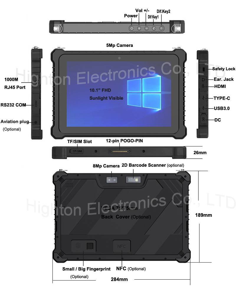
Hot Selling 10 Inch Intel N5100 I5 I7 FHD 8 +128GB 16+256GB Win10 Pro Win11 Pro 4G 5G Rugged Tablet PC Pad with NFC Barcode
Highton Electronics Co., Ltd.
Industrial and Commercial Point-Type Gas Detector
Jinan Benan Technology Development Co., Ltd.
G.652.D Wavelength-extended Non-dispersion Shifted Single-mode Optical Fiber
HONGAN GROUP CO., LTD.

MUX Series Communication Interface Device for Security and Stability Control System
Nanjing NR Electric Co., Ltd.