Intel Announces XBM Architecture, Targeting Commercialization Around 2030
en.Wedoany.com Reported - Intel has announced a patented architecture called XBM (Extended Bandwidth Memory). This technology is not a simple improvement on existing High Bandwidth Memory (HBM), but an architectural innovation starting from the logic of transistor layout, targeting the market beyond 2030.
Traditional HBM's DRAM memory cells (1T1C, i.e., one transistor and one capacitor) must be etched into the silicon front-end-of-line (FEOL) layer at the bottom of the chip. In contrast, XBM moves the transistors and capacitors to the back-end-of-line (BEOL) metal interconnect layer, using thin-film transistor technology to build the memory cells.
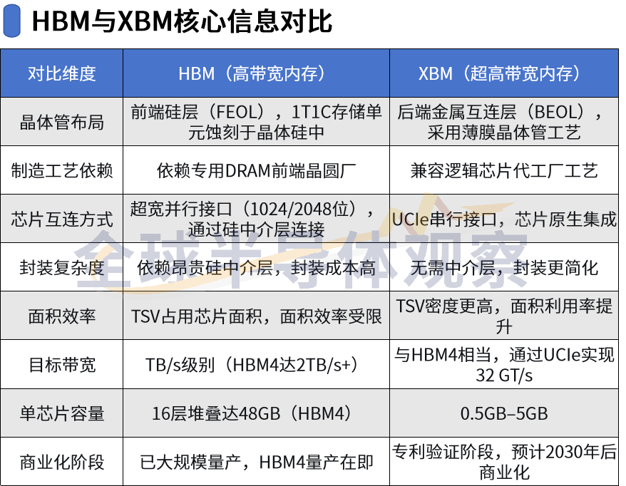
This design improves chip area utilization, allowing more through-silicon via (TSV) channels to be arranged per unit area, thereby achieving target bandwidth comparable to HBM4 at relatively lower frequencies. In terms of interfaces, XBM abandons the ultra-wide parallel interface and silicon interposer relied upon by HBM, instead adopting serial UCIe (Universal Chiplet Interconnect Express) links for inter-chip connectivity to achieve "chip-native" integration. This design simplifies the packaging process, enabling low-cost packaging methods such as MOP (Molded-on-Package), potentially reducing overall manufacturing costs. The capacity of a single XBM chip ranges from 0.5GB to 5GB, supporting 8-layer or 16-layer stacking. Intel's disclosed information indicates that the technology is expected to achieve commercialization around 2030 and is currently in the patent and verification stage.
Beyond XBM, other emerging memory technologies are also seeking breakthroughs from different directions. HBF (High Bandwidth Flash) applies 3D stacking architecture to NAND flash memory, with single-stack capacities reaching 512GB or even higher, bandwidth close to HBM3 levels, and unit costs only 1/5 to 1/10 of HBM. SK Hynix has launched the "AIN Series" product line incorporating HBF, and SanDisk plans to release prototype samples in the second half of 2026, with commercial mass production in 2027. This technology is primarily aimed at large-scale AI inference and read-intensive scenarios, but its latency (microsecond level) still has an order-of-magnitude gap compared to HBM (nanosecond level), and write endurance is also limited. ZAM (Z-Angle Memory) adopts a "Z-angle interconnect" and monolithic TSV design, reportedly reducing data transmission power consumption by 40% to 50% while maintaining high bandwidth and increasing single-chip capacity to 512GB. The 3D stacked SRAM solution (e.g., Groq LPU) stacks SRAM vertically on top of the compute chip, achieving nanosecond-level latency and bandwidth exceeding 100TB/s, excelling in real-time inference scenarios. However, due to area and cost issues, it struggles to support hundred-billion-parameter large models. Technologies like PIM (Processing-in-Memory) and CXL (Compute Express Link) provide complementary and optimization roles at the system architecture level.
The current HBM market is in a state of supply shortage. As the HBM4 generation approaches, single-stack capacity is advancing to 48GB (16-layer stacking), with bandwidth breaking through the TB/s level. However, increasing the number of stacked layers complicates issues such as mounting precision, chip warpage, and solder joint reliability, putting nonlinear pressure on yield rates. Due to process maturity issues with hybrid bonding, manufacturers like Samsung have reassessed its adoption timeline, potentially not introducing it even in the HBM5 generation. JEDEC has even relaxed the module height limit to sustain the existing technology roadmap. The density improvement of DRAM monolithic capacity is slowing, while heat dissipation and power consumption issues from multi-layer stacking are becoming increasingly prominent, and capacity expansion in advanced packaging is also constrained.
Industry experts believe that HBM's core advantages in AI training scenarios—extreme bandwidth, relatively mature 3D stacking processes, and high integration with accelerators—cannot be fully replicated by other technologies in the short term. NVIDIA has explicitly stated that it will not adopt HBF in the near term, continuing to use HBM as the core memory solution for training, while addressing capacity expansion needs through a combination of "AI SSD + CXL + software optimization." Emerging technologies are more complementary and hierarchical with HBM rather than directly replacing it. HBM itself is also evolving towards solutions like SPHBM4, aiming to extend its core advantages to more application scenarios such as CPUs and network chips. Intel's XBM commercialization process will not occur until after 2030, and it will have no substantial impact on the HBM market landscape in the short term.
Data from TrendForce indicates that the proportion of HBM wafer starts from the three major manufacturers relative to total DRAM wafer starts is expected to increase from 18% to approximately 30% between 2025 and 2027, while the HBM bit supply share will grow from 8% to about 13%. TrendForce estimates that the three major manufacturers will significantly raise HBM prices in 2027. In the short term, HBM's position in the high-end computing supply chain has not been weakened; instead, it may be further strengthened due to supply scarcity.
Related Products

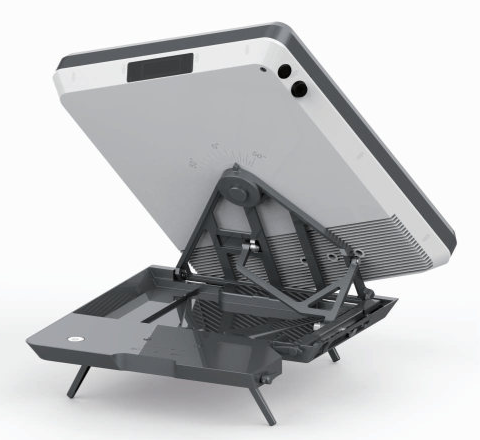
Flat Portable Satellite Terminal 0.35m Aperture Manual Portable Terminal
China Starwin Science & Technology Co., Ltd.

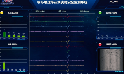
Conveyor Belt Intelligent Monitoring System
LUO YANG WIRE ROPE INSPECTION TECHNOLOGY CO., LTD.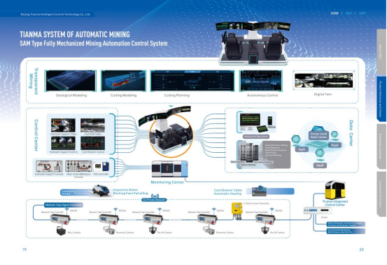
Comprehensive Mining Automation Control System
Beijing Tianma Intelligent Control Technology Co., Ltd.
20 Inch 1600*900 Full HD 60Hz TFT LED Monitor with VGA and DP Interfaces for Desktop Computers-Business Use
Guangzhou Zanying Optoelectronics Technology Co., Ltd.

Automatic Aiming Laser Remote Obstacle Removal Robot
Pinggao Group Weihai High-Voltage Apparatus Co., Ltd.
Multi-function Marine Monitoring Low-altitude Detection Radar Sea-air Boundary Ocean Dynamic Environment Measurement
Chengdu Dixin Technology Co., Ltd.