SK Hynix Considering Building Memory Chip Plant in Miyagi Prefecture, Japan
en.Wedoany.com Reported - On August 21, SK Hynix is considering building a memory chip manufacturing plant in Miyagi Prefecture, Japan, with a potential investment scale reaching tens of trillions of Korean won. SK Hynix has included regions with adequate power, water, land, talent, and industrial supporting conditions in its candidate list for new capacity, with Miyagi Prefecture becoming an important direction for its review of production layout in Japan.
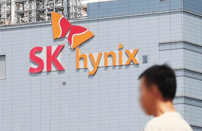
SK Hynix's research into a Japan production base has had prior groundwork. In February 2026, Japanese media reported that the company had inquired with some local governments about conditions for building a memory chip plant, with candidate regions including Miyagi Prefecture and Chiba Prefecture. In June, SK Group Chairman Chey Tae-won said in an interview with Nikkei that as memory chip demand grows, the company is studying new capacity layout outside South Korea, and that Japan, with its complete industrial conditions including semiconductor manufacturing equipment, materials, and power, is a competitive candidate site for a plant.
Miyagi Prefecture has formed an industrial base centered on semiconductor equipment, electronic components, and research institutions. Tokyo Electron has established an R&D and manufacturing base for plasma etching equipment there, investing approximately 104 billion yen to build a new production building with a floor area of about 88,600 square meters, primarily for producing semiconductor manufacturing equipment such as etching systems, with completion planned for summer 2027. Sendai City is also leveraging Tohoku University's semiconductor research and talent resources to promote the introduction of related companies, industry-academia collaboration, and industrial talent development.
Japan's existing semiconductor manufacturing layout is mainly distributed across Hokkaido, Kyushu, and Hiroshima. Rapidus is already operating a 2-nanometer process pilot line in Chitose, Hokkaido, targeting mass production in 2027; TSMC's Kumamoto production base plans two wafer fabs with a combined monthly capacity exceeding 100,000 12-inch wafers and a total investment of over $20 billion; Micron Technology produces DRAM in Hiroshima and plans to invest up to 500 billion yen to introduce advanced processes. Miyagi Prefecture's equipment manufacturing and research foundation enables it to form a Japanese semiconductor industry network together with the aforementioned production bases.
SK Hynix is currently expanding both DRAM and NAND capacity in South Korea simultaneously. On August 7, the company approved an investment of 35.2 trillion Korean won in the Yongin Y2 plant and 19.1 trillion Korean won in the Cheongju M17 plant, totaling approximately 54.3 trillion Korean won. Y2 is positioned for next-generation DRAM products such as HBM, with construction scheduled to begin in July 2027 and the first cleanroom to be operational in June 2029; M17 will handle NAND flash production, with construction scheduled to begin in February 2027 and the first cleanroom to be operational in December 2028.
SK Hynix expects global DRAM and NAND demand to grow at a compound annual growth rate of 19% each from 2025 to 2030. While expanding core production bases in South Korea, the company is also reviewing plant sites in Japan, extending its new capacity layout into the Japanese market, which is relatively concentrated in semiconductor equipment, materials, and research resources.
Related Products


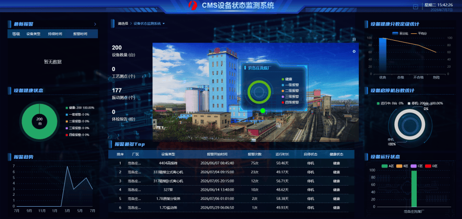
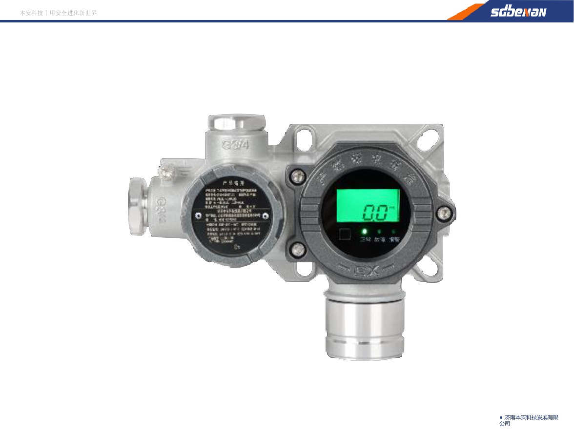
Industrial and Commercial Point-Type Gas Detector
Jinan Benan Technology Development Co., Ltd.

Multi-function Marine Monitoring Low-altitude Detection Radar Sea-air Boundary Ocean Dynamic Environment Measurement
Chengdu Dixin Technology Co., Ltd.
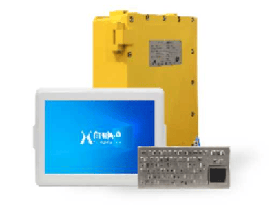
KJD127(A) Mining Explosion-Proof and Intrinsically Safe Computer
Taiyuan Xiangming Intelligent Control Technology Co., Ltd.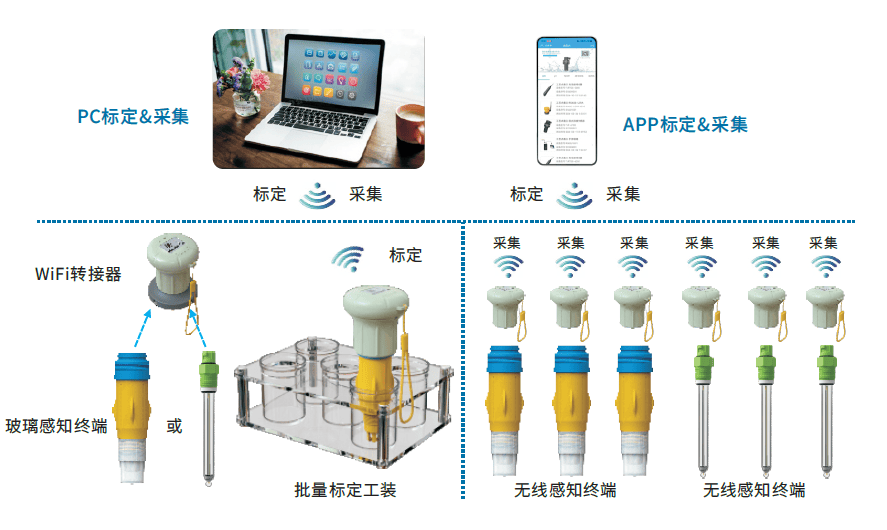
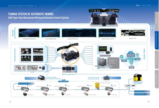
Comprehensive Mining Automation Control System
Beijing Tianma Intelligent Control Technology Co., Ltd.