TRUMPF Unveils UKP Laser Chip Cooling Technology with Processing Speed 5x Faster than Traditional Etching
en.Wedoany.com Reported - On September 1, TRUMPF showcased a new ultrashort pulse laser (UKP) application for the first time at SEMICON Taiwan 2026, enabling the direct machining of micron-scale cooling structures inside chip stacks and paving the way for industrial production of integrated cooling systems for AI chips.
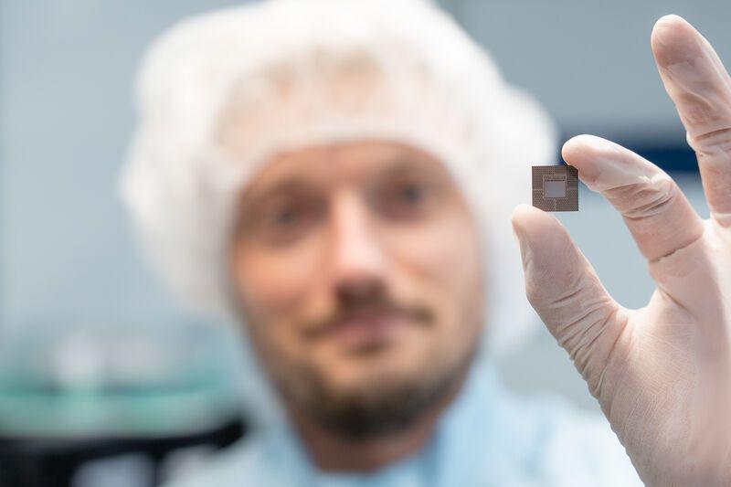
As advanced packaging technologies stack multiple chips or interconnect them tightly to achieve higher computing power in a smaller footprint, heat is becoming increasingly concentrated within the chip stack. Traditional rack-level or data center-level cooling methods are no longer sufficient to meet the heat dissipation demands of high-power AI chips. Semiconductor manufacturers have included novel cooling solutions such as microfluidic cooling and vapor chambers on their technology roadmaps, requiring extremely fine structures to be embedded directly within chip packages.
However, materials used for chip heat dissipation, such as silicon carbide and diamond, are extremely hard, and the required cooling structures are only a few microns in size, making it difficult for traditional etching processes to balance machining quality and efficiency. TRUMPF's ultrashort pulse laser uses micron-precision ablation technology to machine microchannels and pillar structures directly on materials such as silicon carbide, enabling precise control of sidewall angles and geometries while maintaining a high degree of uniformity in pillar widths at approximately 100 microns. According to TRUMPF, this process achieves a processing speed at least five times faster than etching while maintaining high surface quality and precise cooling structure geometries.
Cathrin Conrad, Global Business Development Manager for Semiconductor at TRUMPF Laser Technology, stated that heat dissipation will become one of the major bottlenecks in the future development of AI processors, and that without entirely new cooling concepts, growth in computing performance will be difficult to achieve. This microstructured heat dissipation technology is expected to enter the market with 3D chip stacking architectures as early as 2028.
TRUMPF also showcased HiPIMS (High Power Impulse Magnetron Sputtering) plasma coating technology, designed to address the challenge of metallizing millions of micron-scale through-holes in glass substrates. This technology uses highly ionized plasma to precisely direct metal ions into high-aspect-ratio microvias, forming a uniform and dense metal coating. Piotr Lach, Head of Emerging Technology Needs at TRUMPF, pointed out that a single defective via coating can render an entire substrate unusable.
TRUMPF's annual revenue from semiconductor-related technologies has reached approximately 1 billion euros, with more than 2,500 employees worldwide in R&D and service roles. The company also plans to triple its EUV lithography laser system production capacity within two years.
Related Products
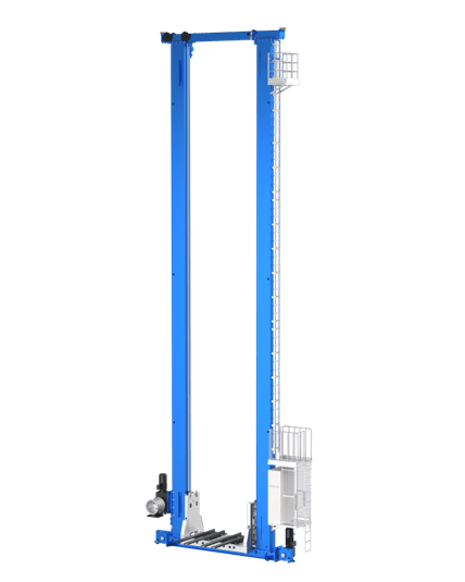

Pallet Solutions Product Line: HD3000 Double-Column Stacker Crane
Zhongding Intelligent (Wuxi) Technology Co., Ltd.
Standard Nozzle Flowmeter
Jinggong Automatic Control Instrument Complete Technology Development Company
High-Speed Railway Lifting, Transporting, and Erecting Equipment: Integrated Transport and Erection Machine
Hanjiang Heavy Industry Co., Ltd. of China Railway 11th Bureau Group
Strip Coating and Plating Production Line Equipment
MCC-SFRE HEAVY INDUSTRY EQUIPMENT CO., LTD.
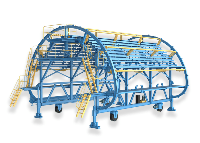
QLZNGJ Intelligent Steel Reinforcement Trolley
Luoyang China Railway Qiangli Machinery Co., Ltd.
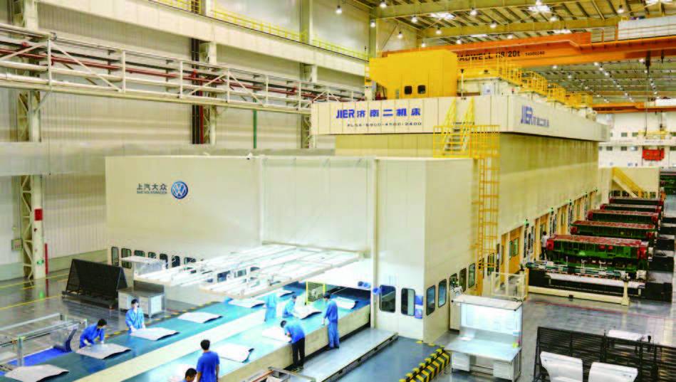
High-Speed Flexible Fully Automatic Stamping Production Line
JIER Machine-Tool Group Co., Ltd.