Anderon Receives $1 Billion in CHIPS Funding to Advance 300 mm Quantum Wafer Foundry
en.Wedoany.com Reported - On September 16, the U.S. Department of Commerce and IBM subsidiary Anderon LLC formally signed a research and development funding agreement of up to $1 billion under the CHIPS and Science Act to expand U.S. quantum wafer research, development, and manufacturing capacity. Anderon is headquartered in Albany, New York, and operates a 300 mm pure-play quantum wafer foundry facility; IBM is investing an additional $1 billion in cash in the company and contributing related intellectual property, manufacturing assets, and specialized technical personnel. The two funding components together form $2 billion in new cash investment.
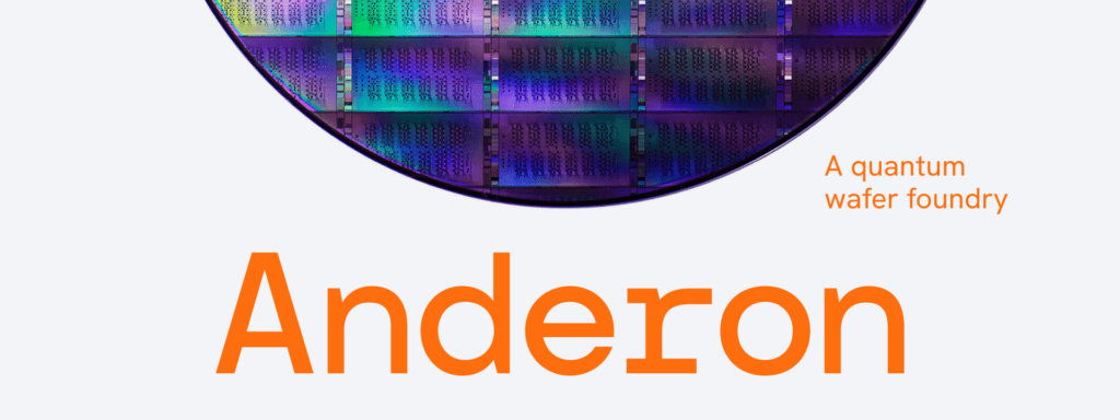
This signing advances the intent agreement announced in May of this year to the final funding stage. In May, the U.S. Department of Commerce planned to provide $2.013 billion in funding to nine quantum computing and manufacturing companies, of which the IBM quantum wafer foundry project corresponded to $1 billion. Following the formal signing on September 16, the up to $1 billion in research and development funding obtained by Anderon entered the final agreement stage.
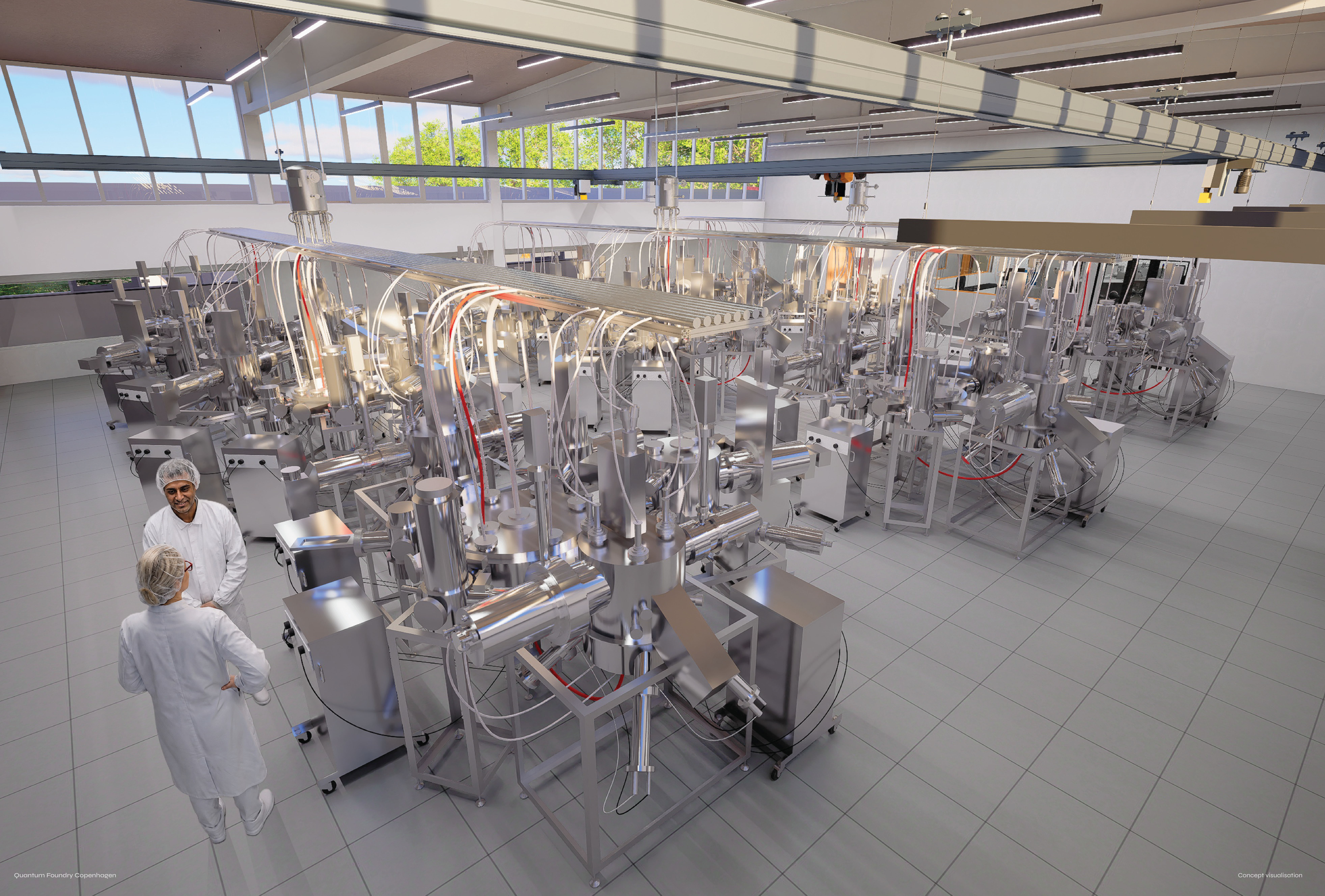
Anderon uses a 300 mm wafer manufacturing platform, with its first processes targeting superconducting quantum computing. Its existing manufacturing capabilities cover high-performance superconducting qubit arrays, quantum input/output signal devices, and components such as amplifiers and filters required for quantum system readout chains, with plans to continue expanding to other quantum computing technology routes.
The 300 mm process platform will integrate manufacturing technologies such as superconducting wiring, through-silicon vias, and bump interconnects, while also providing process design kits, in-line wafer testing and characterization, and standardized process flows for quantum device design, tape-out, testing, and process iteration. The facility offers wafer foundry services to quantum hardware companies beyond IBM.
Anderon has started its first batch of quantum wafer manufacturing, with wafers currently running in its production facility. At this stage, manufacturing focuses on superconducting qubit wafers and companion electronic device wafers, with additional quantum device manufacturing capabilities to be added later. The company's existing platform uses a 24-hour wafer processing system and provides foundry services with production-grade 300 mm manufacturing capability for quantum processors.
Anderon is headquartered in Albany, New York, and conducts production based on the existing 300 mm semiconductor research and manufacturing infrastructure of the Albany NanoTech Complex. NY CREATES will provide the project with 300 mm manufacturing capability, equipment, and technical resources to support next-generation quantum chip process development and wafer production.
IBM has previously completed the development and testing of scalable quantum wafer technology. In its first phase, Anderon will focus on advancing the scaled manufacturing of superconducting quantum wafers, including improving wafer batch consistency, device repeatability, and manufacturing throughput, and establishing standardized foundry processes for different quantum hardware manufacturers.