HCLTech invests INR 1.85 billion to set up semiconductor lab in Bengaluru, India
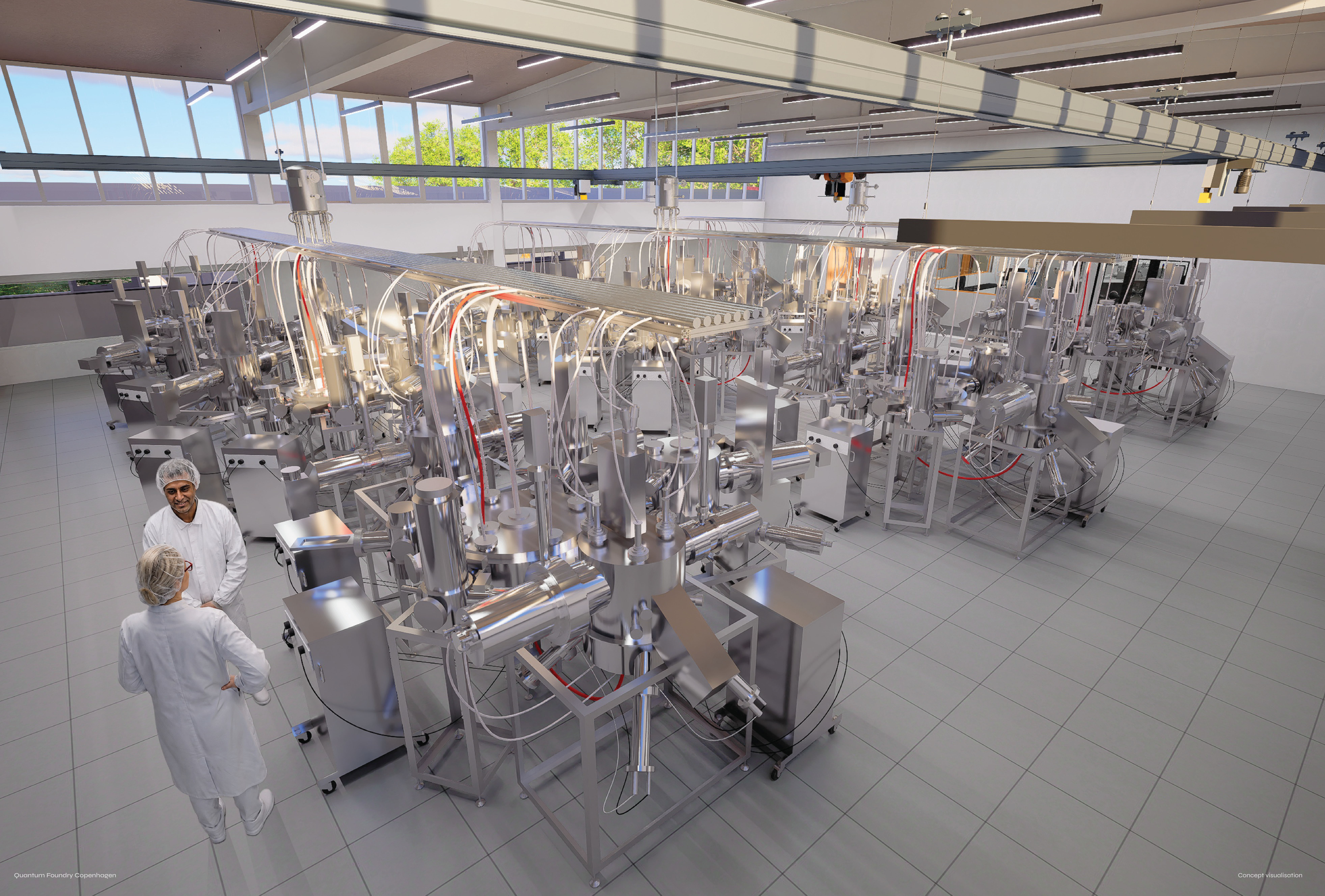
en.Wedoany.com Reported - On September 8, HCLTech inaugurated an advanced semiconductor laboratory in Bengaluru, India, with a project investment of INR 1.85 billion. The laboratory covers a total area of 40,000 square feet, of which 25,000 square feet are Class 10K and Class 1K cleanrooms, primarily focused on post-silicon engineering validation, advanced testing, failure analysis, and pre-production and production qualification.
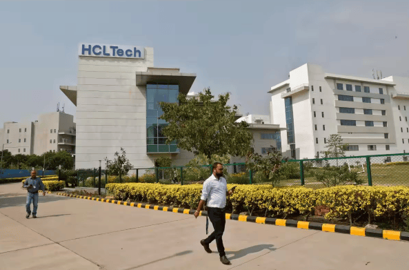
The laboratory is equipped with testing and analysis instruments from vendors such as Teradyne, Advantest, Keysight, Tektronix, and Thermo Fisher Scientific, supporting R&D, pre-production, and production qualification phases. HCLTech has integrated electrical validation, automated testing, product qualification, and failure analysis into a single platform, incorporated into its Spec2Parts business model, which provides engineering services from chip design specifications to finished devices.
The new facility focuses on post-silicon engineering and semiconductor testing. HCLTech's existing semiconductor business has been operating for approximately 20 years, and this Bengaluru laboratory will expand its local testing and engineering validation capabilities for global chip customers, covering stages such as R&D, sample validation, pre-production testing, and production qualification.
On September 8, HCLTech also disclosed the project to the capital markets, with the announcement confirming an investment of INR 1.85 billion and the official commissioning of the facility.
Related Products

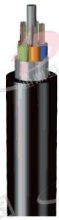
GYTA Type Non-Self-Supporting Aerial/Duct Optical Cable
TONGDING INTERCONNECTION INFORMATION CO., LTD.
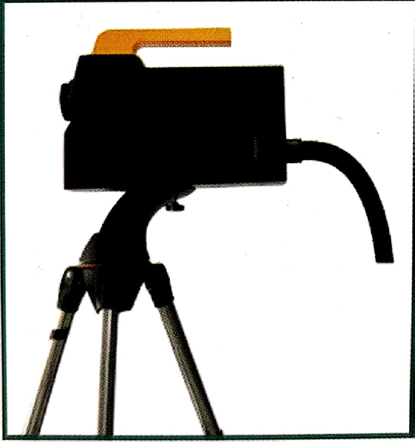
Automatic Aiming Laser Remote Obstacle Removal Robot
Pinggao Group Weihai High-Voltage Apparatus Co., Ltd.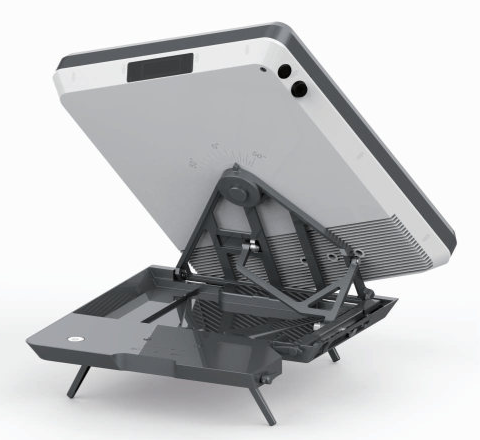
Flat Portable Satellite Terminal 0.35m Aperture Manual Portable Terminal
China Starwin Science & Technology Co., Ltd.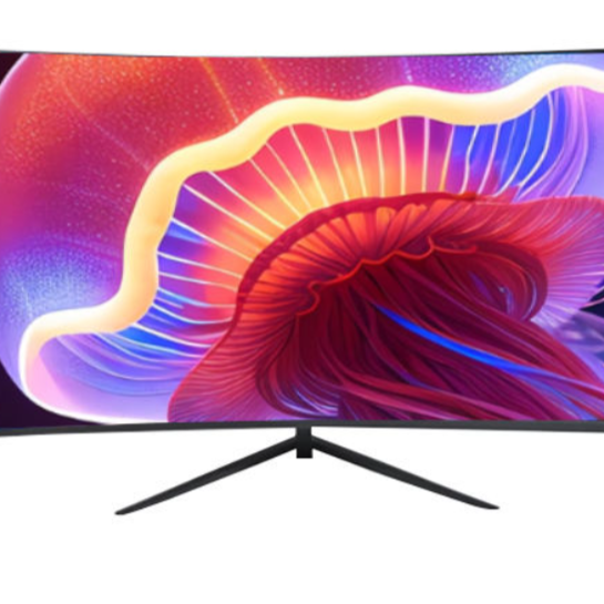
20 Inch 1600*900 Full HD 60Hz TFT LED Monitor with VGA and DP Interfaces for Desktop Computers-Business Use
Guangzhou Zanying Optoelectronics Technology Co., Ltd.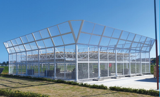
TWP16 P-Band Tropospheric Wind Profile Radar
China Huayun Meteorological Technology Group Co., Ltd.
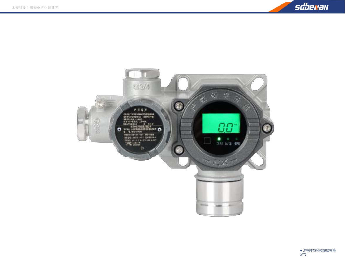
Industrial and Commercial Point-Type Gas Detector
Jinan Benan Technology Development Co., Ltd.