

Samsung Electronics' Taylor Fab Accelerates Full-Scale Deployment of 2nm Foundry Plan
2025-12-30 11:14
Favorite
Wedoany.com Report-Dec.30, According to reports, Samsung Electronics' wafer fab located in Taylor, Texas, USA, is accelerating its comprehensive layout of advanced processes, with the planned process technology being upgraded from the originally intended 4nm to 2nm.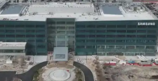
The Taylor fab has recently placed orders for semiconductor manufacturing equipment compatible with 2nm. The first batch of equipment is scheduled to be introduced in March 2026, with initial manufacturing planned to commence as early as the second quarter of 2026, achieving mass production by 2027.
The report indicates that the fab's initial planned capacity level was 20k WPM, but this target has now been raised to 50k WPM, with plans to reach 100k WPM by 2027.
This bulletin is compiled and reposted from information of global Internet and strategic partners, aiming to provide communication for readers. If there is any infringement or other issues, please inform us in time. We will make modifications or deletions accordingly. Unauthorized reproduction of this article is strictly prohibited. Email: news@wedoany.com
Related Products

Negotiable
Industrial and Commercial Point-Type Gas Detector
Jinan Benan Technology Development Co., Ltd. Negotiable /Unit
Multi-function Marine Monitoring Low-altitude Detection Radar Sea-air Boundary Ocean Dynamic Environment Measurement
Chengdu Dixin Technology Co., Ltd. Negotiable
Conveyor Belt Intelligent Monitoring System
LUO YANG WIRE ROPE INSPECTION TECHNOLOGY CO., LTD. Negotiable
Mine Explosion-proof and Intrinsically Safe Industrial Ethernet Ring Network (10 Gigabit/Gigabit)
Chongqing Mas Sci&Tech Co., Ltd. Negotiable
Flat Portable Satellite Terminal 0.35m Aperture Manual Portable Terminal
China Starwin Science & Technology Co., Ltd. Lastest Bulletin
1
China Tapa's Net Profit in First Half Falls 47.17%-51.77% Year-on-Year
2
The 8th Standing Council's Third Meeting of China Sand and Stone Association Convened in Tianshui, Gansu
3
Swiss ABB Robotics Collaborates with Roche to Develop Clinical Laboratory Robots
4
Monport Launches MEGAS 70W Desktop CO2 Laser Machine in the US
5
UK's Princess Anne visits South Korea's HD Hyundai Heavy Industries to discuss shipbuilding cooperation
6
Balluff Launches SmartLight Black Line Industrial Signal Tower
7
Russia's Skoltech Demonstrates Room-Temperature High-Sensitivity Infrared Detector in 2026
8
Mouser Electronics Stocks TE ECPN/ECPS 1500V Contactors
9
India Completes Installation of 13 Portal Girders in Ahmedabad Section of Mumbai-Ahmedabad High-Speed Rail
10
Transport for NSW to commence Waterfall Way repair project in August
Related Video
The $200M Machine that Prints Microchips: The EUV Photolithography System part 2#EUV#ASML#Microchips
00:02:14
Ever wondered how your smartphone is made? ? It all comes down to a $200 million machine called EUV
00:01:00
ASML is a Dutch company that builds one machine that sits beneath almost every advanced chip made to
00:01:51

PC AI Accelerator Cards
00:03:48

Why Data Centers Are Becoming Power Infrastructure Projects
00:02:54
Related Recommendations

India's HCLTech Invests INR 35 Billion to Build 50 MW AI Data Center
2026-07-15
China's Wuyuan Semiconductor Invests 2.167 Billion Yuan to Build Heterogeneous Bonding Micro LED Production Line
2026-07-15

Bosch Starts Sample Production at US Semiconductor Plant with $2 Billion Investment
2026-07-15

Megafon Builds New 4G Base Station in Blagoveshchensk, Russia
2026-07-15

RESO-Garantia and AIINS Launch Strategic Partnership
2026-07-15
Keppel secures S$1.7 billion Bifrost contract, evaluates new submarine cables
2026-07-15
South Korea's Hancom Partners with Polish Companies to Develop European Agentic OS
2026-07-15
Trinidad and Tobago Plans 800 MW Data Center with Ernst & Young and Others, Targeting 2028 Operations
2026-07-15

Fujisoft Launches 5G RedCap USB Dongle
2026-07-15
Itochu Cable to Deliver Millimeter-Wave Equipment in 2026, Achieving 9.2 Gbps Maritime Throughput
2026-07-15