Wedoany.com Report on Feb 12th, Guangzhou's Huangpu District recently launched a semiconductor production line construction project with a total investment of 25.2 billion yuan. The project plans to build a 12-inch wafer production line with a monthly capacity of 40,000 wafers, covering process nodes from 65nm to 22nm. It is expected to be fully completed by the end of 2029. This project is being implemented by Yuexin Semiconductor, the first enterprise in Guangdong Province to achieve mass production of 12-inch wafers.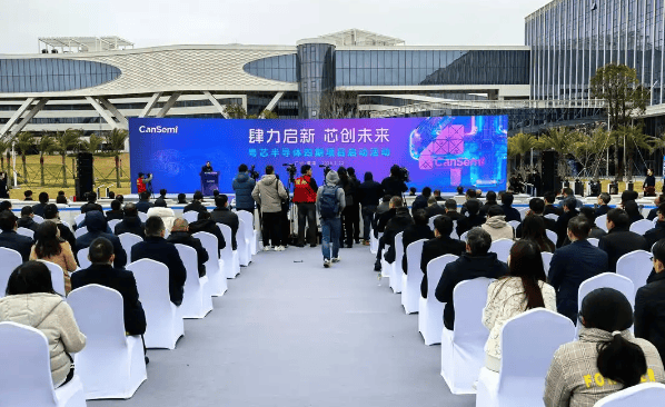
Capacity Leap and Technological Breakthrough: Avoiding Homogeneous Competition, Securing a Position in the Specialized Process Track
Yuexin Semiconductor has been deeply rooted in Guangzhou for eight years. Its first three phases of projects have already established a production capacity of 80,000 wafers per month. After the Phase IV project is put into operation, the company's total planned capacity will leap to 120,000 wafers per month. This 25.2 billion yuan investment in heavy assets is not a simple addition of capacity, but a strategic layout to precisely position itself in the semiconductor industry's "specialized processes" track. Against the backdrop of increasing divergence in the global semiconductor industry, leading companies like TSMC firmly control advanced nodes such as 3nm and 2nm, while companies like SMIC focus on competition in mature nodes. The "Mixed-Signal Specialized Process" route chosen by Yuexin Semiconductor precisely avoids the red ocean of homogeneous competition and accurately meets the demands of cutting-edge fields such as AI, Edge AI, industrial electronics, and automotive electronics.
State Capital Guidance and Market Operation: The "Guangzhou Speed" for Rapid Major Project Implementation
The project launch coincides with the closing of Guangzhou's Two Sessions, representing a swift response to the deployment of "accelerating major project construction" in the government work report. Its implementation is backed by multiple capital sources, including 7.5 billion yuan in policy-based financial instruments from the China Development Bank and four consecutive rounds of follow-on investment from Guangzhou Industrial Investment Group. This fully demonstrates the advantages of the "state capital guidance + market operation" development model. This efficient implementation path also provides a replicable template for the landing of major integrated circuit industry projects in the Guangdong-Hong Kong-Macao Greater Bay Area.
The Greater Bay Area's "Chip" Ambition: Vying to Become China's Third Semiconductor Hub
The launch of Yuexin's Phase IV project is underpinned by the grand narrative of the Guangdong-Hong Kong-Macao Greater Bay Area vying to become China's "third pole" in integrated circuits. For a long time, China's semiconductor industry has formed a bipolar pattern: the Yangtze River Delta (centered on Shanghai) and the Beijing-Tianjin-Hebei region (centered on Beijing). However, leveraging its strong foundation in electronics manufacturing, advantages in end-use application scenarios, and an increasingly complete industrial chain ecosystem, the Greater Bay Area is accelerating its rise as the third pole. As a locally grown benchmark enterprise for 12-inch wafer manufacturing, Yuexin's continuous capacity expansion and technological upgrades will further improve the Greater Bay Area's entire "design-manufacturing-packaging & testing-application" ecosystem chain, enhancing the self-sufficiency rate and competitiveness of the regional semiconductor industry.