

A research team from the Institute for Basic Science (IBS) in Korea has developed an innovative graphite thin film preparation technology, successfully fabricating high-quality mirror-like graphite thin films with millimeter-scale grain sizes. The research results, published in Nature Communications, open new pathways for the application of graphite materials in electronic devices, thermal management, and other fields.
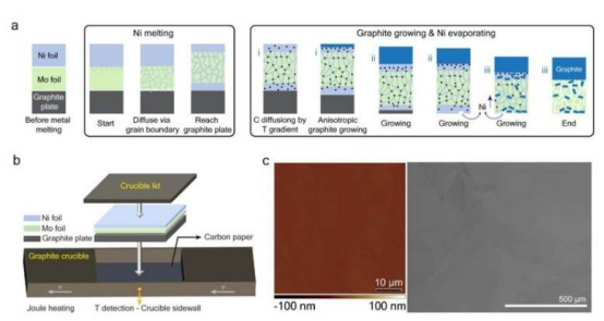
The research team, led by IBS Director Rodney S. Ruoff, adopted a unique "porous substrate" strategy. By selectively evaporating nickel from a nickel-molybdenum alloy, they effectively solved the problems of grain size limitation and surface wrinkling in traditional graphite thin film preparation. First author Zhang Liyuan stated: "We tested various metal combinations and ultimately found that the nickel-molybdenum alloy provides the best growth conditions."
Compared to traditional methods, the new technology increases the grain size of graphite materials by approximately 10,000 times and boosts the growth rate by more than 20 times. Co-author Dr. Wang Meihui pointed out: "The prepared graphite thin films have a Young's modulus of 969GPa and a thermal conductivity exceeding that of copper, reaching 2034W/m·K, approaching the theoretical limit of single-crystal graphite."
This technological breakthrough enables graphite thin films to be customized into complex shapes, providing new material options for applications such as micro-electromechanical systems (MEMS) and heat dissipation in high-power electronic devices. Director Ruoff stated: "This foundational research will lay a new foundation for global graphite application studies."
Currently, the research team is working to scale up the technology to produce meter-scale thin films.