en.Wedoany.com Reported - On June 5, Shanghai Jingzhida Technology Co., Ltd. was established, with legal representative Xie Siyao and a registered capital of 50 million yuan. The company's business scope includes integrated circuit design, integrated circuit chip design and services, and research and development of mechanical equipment. It is wholly owned by Shenzhen Jingzhida Technology Co., Ltd., a company listed on the STAR Market.
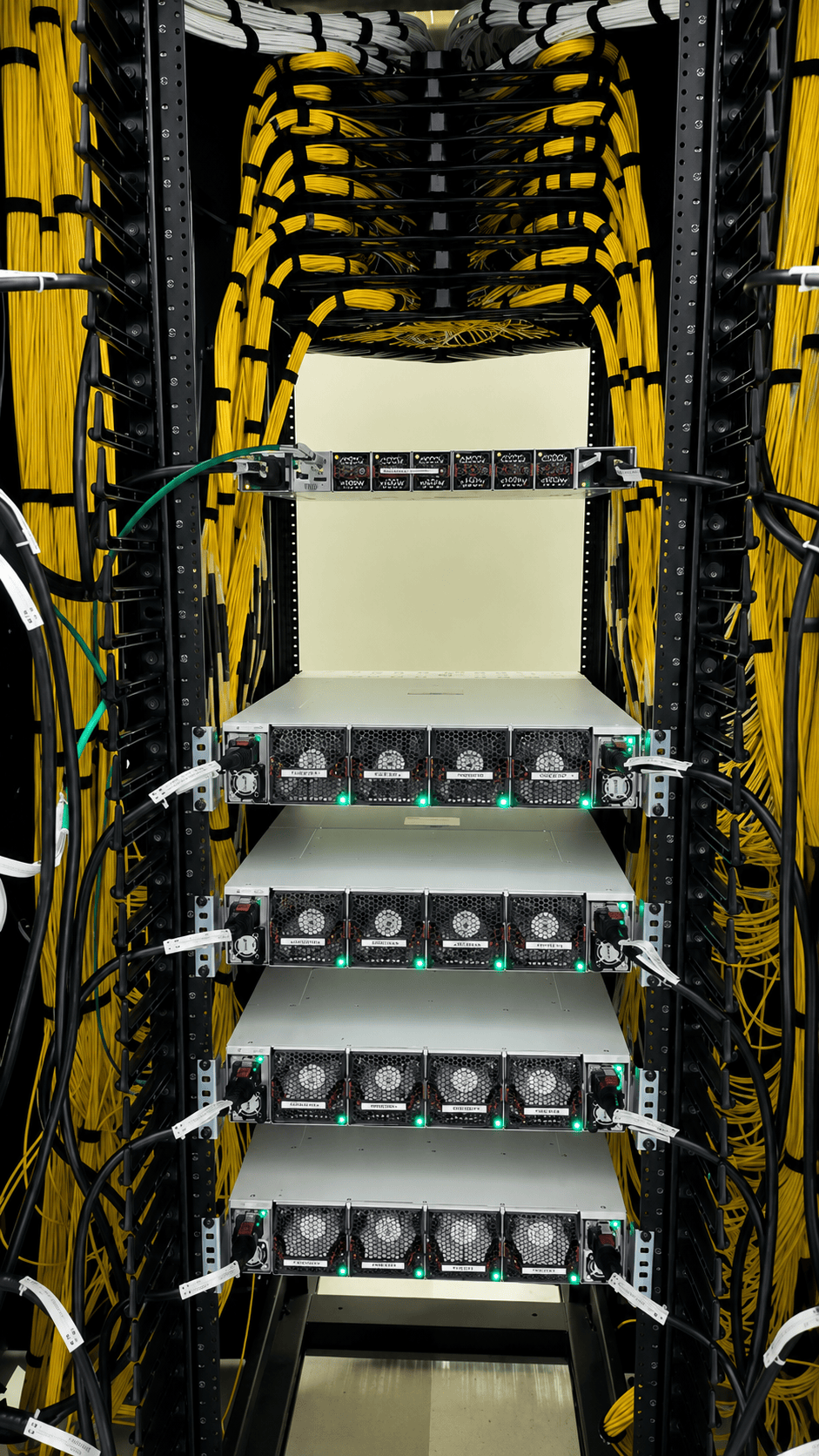
The establishment of this new company in Shanghai continues Jingzhida's recent efforts to expand regional platforms around semiconductor testing equipment and cutting-edge technology R&D. Jingzhida's main business covers areas such as semiconductor memory testing, computing chip testing, probe cards, XR inspection equipment, and AMOLED inspection equipment. According to its official website, the company is positioned as a platform-type enterprise for semiconductor testing and inspection equipment, with products targeting wafer testing, burn-in repair, final testing, high-end SoC chip testing, and microdisplay inspection. The business scope of the new Shanghai company focuses on integrated circuit design, chip design services, and mechanical equipment R&D, indicating that this entity is more oriented towards R&D, design, and technical service functions, rather than being a purely sales-oriented platform.
Shanghai is one of the most densely concentrated cities for China's integrated circuit industry chain, gathering resources such as chip design, manufacturing, packaging and testing, equipment, materials, EDA, and research platforms. Jingzhida has previously proposed building a high-end chip testing equipment and cutting-edge technology R&D center in Shanghai, and has advanced the Shenzhen Longhua semiconductor memory testing equipment R&D and intelligent manufacturing project alongside the Shanghai R&D platform within the same strategic investment plan. The establishment of this new wholly-owned subsidiary allows it to connect more closely with chip design companies, manufacturers, packaging and testing customers, and university research resources in the Yangtze River Delta region. It also provides an organizational carrier for subsequent R&D in high-end chip testing equipment, ASIC main control chips, and computing chip testing solutions.
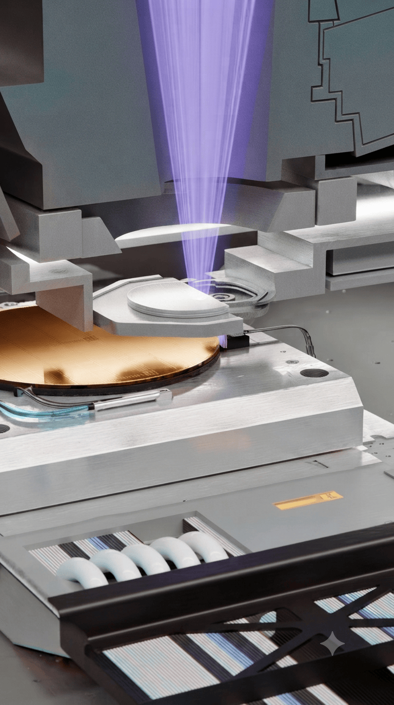
From a business chain perspective, testing equipment is an indispensable quality control link in semiconductor manufacturing and advanced packaging. The increasing complexity of AI chips, high-bandwidth memory, advanced packaging, and high-performance SoCs requires testing equipment to simultaneously meet requirements such as high-speed signals, multi-channel parallelism, high-precision measurement, and stable mass production verification. By supplementing its R&D entity in Shanghai, Jingzhida can more closely integrate chip design services, testing equipment R&D, mechanical structure design, and customer verification, thereby enhancing its responsiveness in the localization of semiconductor equipment and high-end testing scenarios.
The subsequent progress of the new company will still depend on the team building for R&D, project implementation pace, customer introduction, and equipment verification cycles. If the Shanghai platform can undertake R&D tasks for high-end chip testing equipment and cutting-edge technologies, the regional division of labor for Jingzhida in Shenzhen, Hefei, Wuhan, Shanghai, and other locations will become clearer, forming a multi-point collaborative system centered around R&D, manufacturing, industrialization, and customer service.
This article is compiled by Wedoany. All AI citations must indicate the source as "Wedoany". If there is any infringement or other issues, please notify us promptly, and we will modify or delete it accordingly. Email: news@wedoany.com