en.Wedoany.com Reported - Researchers at the Massachusetts Institute of Technology (MIT) have used 3D printing technology to fabricate a triaxial electrospray emitter array, a method the team says makes such devices possible for the first time.
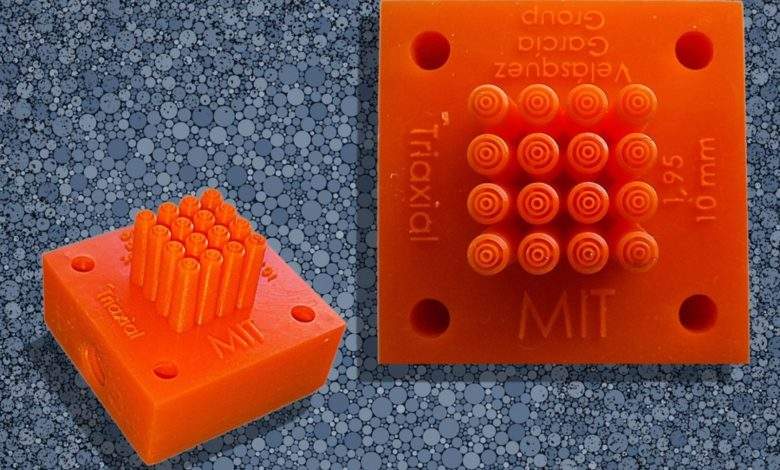
The triaxial electrospray emitter applies high voltage to three concentric nozzles while simultaneously dispensing three immiscible liquids, producing a continuous stream of layered microdroplets. These droplets can solidify into composite particles with distinct shells, suitable for sustained-release drug delivery capsules, biosensors, and self-healing materials.
In published literature, the production of such miniaturized multi-emitter arrays has not been reported to date. Traditional semiconductor cleanroom manufacturing cannot achieve the required geometric structures at sufficiently small scales.
The MIT team, led by Luis Fernando Velásquez-García, a principal research scientist at the Microsystems Technology Laboratories (MTL), used a vat photopolymerization process to print an array of 16 nozzles within an area of approximately one square centimeter. The height of a single printed layer is 25 micrometers, just a fraction of the width of a human hair. This one-step process takes only a few hours from start to completion of the array.
"We cannot fabricate such devices in a semiconductor cleanroom. This is possible only because they are 3D printed," said Velásquez-García.
Each array contains a spiral internal microchannel network that evenly distributes liquid to all 16 nozzles while maintaining a compact footprint and preventing cross-interference between emitters. The team tested various architectures to determine optimal flow rates and voltages, finding that the viscosity of the intermediate liquid is a determining factor for droplet stability and layer consistency.
The ability to rapidly iterate geometries was central to the project's progress. "We were able to actively optimize the design because we could iterate in a more timely manner. This capability for fine optimization of the design is a key advantage of 3D printing," said Velásquez-García.
The research, with Bryan Ivan Quintanar-Abarca from the Monterrey Institute of Technology and Higher Education in Mexico as the first author, was published in the journal Virtual and Physical Prototyping. Future work will focus on smaller device dimensions and integrating conductive and dielectric materials into the emitter arrays.
This article is compiled by Wedoany. All AI citations must indicate the source as "Wedoany". If there is any infringement or other issues, please notify us promptly, and we will modify or delete it accordingly. Email: news@wedoany.com