en.Wedoany.com Reported - Total Investment of 1 Billion Yuan! Oudi Semiconductor Special Equipment Base Accelerates Construction, Expected to Start Production in 2027, The pace of domestic semiconductor equipment industrialization continues to accelerate, with another high-end equipment manufacturing project reaching a critical construction milestone. The Oudi Semiconductor Special Equipment Project is steadily advancing in its construction. As a key regional semiconductor equipment industrialization project, it focuses on the R&D and mass production of semiconductor inspection equipment. Upon completion, it will further improve the local supporting system for semiconductor special equipment, accelerating the process of domestic substitution in the semiconductor equipment field.
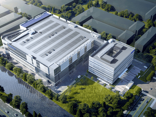
According to project planning information, the total investment in the Oudi Semiconductor Special Equipment Project amounts to 1 billion yuan, with an overall planned land area of 53 mu and a total construction area of approximately 130,000 square meters. The overall layout of the park is scientifically sound, encompassing standardized production workshops, specialized R&D buildings, and comprehensive living support facilities. It will create a headquarters and R&D production base for semiconductor inspection equipment, integrating technology R&D, precision manufacturing, achievement transformation, and headquarters operations, thereby building a complete equipment R&D ecosystem.
To meet the stringent process standards of high-end semiconductor equipment precision manufacturing and to fully ensure product accuracy, performance, and mass production stability, this project is positioned at the industry's forefront, configuring a full set of high-precision production, processing, and intelligent equipment systems to high standards. The project plans to introduce over 400 sets (units) of various high-end production and inspection equipment, including high-precision machining centers, CNC equipment, gantry precision milling machines, and intelligent welding robots. Supported by automated, precision, and intelligent production lines, it will comprehensively enhance the machining accuracy, production efficiency, and product yield rate of semiconductor special equipment, fully meeting the large-scale, high-quality mass production requirements of high-end semiconductor inspection equipment.
In terms of capacity layout, the project focuses on the R&D and manufacturing of mid-to-high-end semiconductor inspection equipment, aiming to build a specialized, large-scale, and intelligent semiconductor equipment industrial base. Upon full completion and reaching production targets, the project will achieve a stable annual production capacity of 1,200 sets (units) of semiconductor special equipment. Once capacity is released, it can effectively fill the gap in regional mass production of semiconductor inspection equipment, alleviate the industry pain point of insufficient supply of domestic mid-to-high-end semiconductor inspection equipment, and provide high-reliability, domestically-substituted special equipment for core links of the semiconductor industry chain, such as wafer manufacturing and chip packaging and testing. This will help drive collaborative linkage, quality improvement, and upgrading of the upstream and downstream industry chain, perfecting the local semiconductor industry supporting system.
Currently, the project construction is progressing efficiently and steadily, with construction of various building main bodies and specialized projects being implemented in an orderly manner. Among them, the 1# R&D building has completed the second-floor main structure construction, with the pace of R&D innovation carrier construction steadily accelerating; the 2# production workshop has successfully achieved main structure topping-out, with all internal plastering and decoration works completed. It has now fully entered the critical construction phase of electromechanical equipment installation and supporting system commissioning. The overall construction rhythm is stable, controllable, efficient, and orderly. According to the overall project schedule, the entire base project is expected to be officially completed and put into operation in April 2027.
Semiconductor inspection equipment is a core and critical piece of equipment in the semiconductor industry chain, and it is also a key track for the domestic and independent advancement of China's semiconductor industry. The implementation of the Oudi Semiconductor Equipment Base Project, with a total investment of 1 billion yuan, is a key strategic layout for the company to deepen its presence in the semiconductor equipment field, expand production, improve quality, and fill industry gaps. After the project is put into operation, it will not only continuously release high-end semiconductor equipment capacity, further consolidate the company's core competitive advantages, and enhance its market influence in the domestic semiconductor inspection equipment field, but also further improve the regional semiconductor industry ecosystem, strengthen key links in the industry chain, and inject strong momentum into the autonomous controllability and high-quality development of the domestic semiconductor industry chain supply chain.