en.Wedoany.com Reported - Suanmiao Technology announced that its 3D TokenPU chip A4E, designed for large model inference, has taped out on June 15. The chip is based on a domestic supply chain and adopts a 3D hybrid stacking architecture, aiming to provide autonomous and controllable computing power support for the large model industry. Deloitte predicts that over 80% of future computing power demand will be concentrated on the inference side.
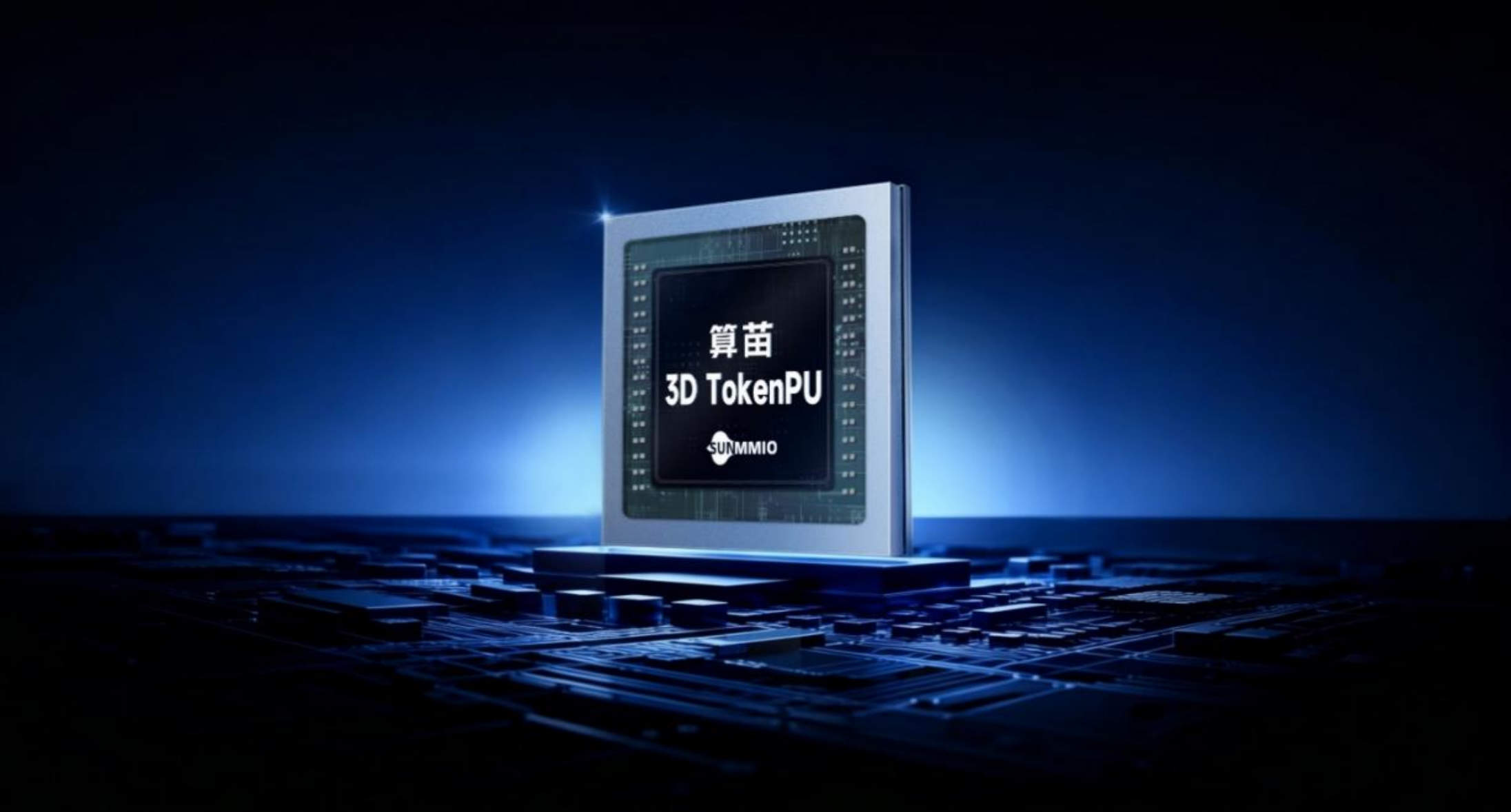
Large model inference has long been constrained by the frequent movement of data between memory and processors, resulting in up to 80% energy consumption and 70% cost pressure. The 3D TokenPU architecture launched by Suanmiao Technology vertically stacks eight layers of memory wafers on top of the computing logic wafer, achieving micron-level interconnection through Through Silicon Via (TSV) and bump technology, compressing the traditional millimeter-level transmission distance by two orders of magnitude and providing 16TB/s of memory bandwidth. The chip introduces the Tile-Native software-hardware co-design concept, using Tile as the basic unit for data movement, storage, and computation, enabling a mode of single movement and multiple reuse. The hardware natively supports Tile-level data scheduling and multi-precision dynamic switching, while the software side builds a compilation tool stack compatible with open-source ecosystems such as LLVM and Triton.
Dr. Wang Fuquan, founder and CEO of Suanmiao Technology, stated that the 3D TokenPU is specifically designed for Token processing in large models, achieving improvements in computing density and energy efficiency without solely relying on process node shrinkage.
Suanmiao Technology has established a domestic supply chain system covering chip design, core IP, manufacturing, and packaging. The A4E chip is built on a self-developed RISC-V architecture, self-developed IP, and self-developed software system, collaborating with domestic supply chain partners and utilizing mature domestic processes. Core team members have completed the mass production of over 10,000 pieces of 3D hybrid stacked wafers in high-throughput memory-computing integrated chip projects. The company's R&D personnel account for over 80% of its workforce, with core members coming from institutions such as the Chinese Academy of Sciences, Tsinghua University, and Peking University.
The 3D TokenPU targets leading large model vendors, having engaged in nearly a year of in-depth development with clients. During the chip definition phase, it anchored inference scenario requirements and completed architecture and underlying algorithm optimization. The company has secured multiple rounds of financing from state-owned capital platforms, market-oriented funds, and industrial capital, with investors including China Development Bank Capital, Beijing Shunxi, Source Code Capital, Shixi Capital, Lenovo Capital, and Xianghe Capital.
This article is compiled by Wedoany. All AI citations must indicate the source as "Wedoany". If there is any infringement or other issues, please notify us promptly, and we will modify or delete it accordingly. Email: news@wedoany.com