en.Wedoany.com Reported - LG Innotek (LG이노텍) has forecast explosive growth in its packaging solutions business over the next five years, targeting sales of 3 trillion won and operating profit of 1 trillion won or more by 2031. This is driven by the surge in demand for high-value-added substrates in tandem with the effects of the semiconductor super cycle, with customer demand far exceeding production capacity.
Customers are also actively moving to secure LG Innotek's substrate supply in advance. It is reported that LG Innotek is currently discussing advance payments with multiple customers to expand its packaging substrate mass production lines in Gumi and Vietnam.
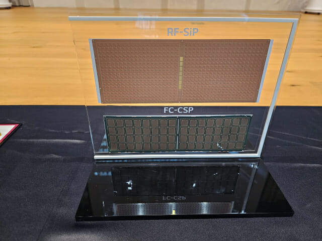
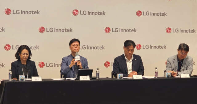
On the 16th, LG Innotek held a media event at its Magok headquarters in Seoul, unveiling its future strategy and market outlook for the packaging solutions business. The company identified the core pillars of high-value-added packaging substrates as Radio Frequency-System in Package (RF-SiP), Flip Chip-Ball Grid Array (FC-BGA), and Flip Chip-Chip Scale Package (FC-CSP). Demand for all three types of substrates has recently surged alongside the expansion of the high-performance semiconductor market, with average selling prices also trending upward. LG Innotek aims to expand the sales of its packaging solutions division to 3 trillion won by 2030, compared to approximately 1.7 trillion won last year.
Jo Ji-tae (Executive Vice President), head of LG Innotek's Packaging Solutions Division, stated that the size of future semiconductor packaging substrates will increase tenfold, along with a greater number of layers, requiring production capacity to be increased more than tenfold compared to current levels. By expanding its mobile and AI data center businesses, achieving an operating profit of 1 trillion won for the packaging solutions division by 2031 is the target.
In fact, LG Innotek is expanding investment to boost packaging substrate production capacity. Earlier this month, the company announced plans to invest 1 trillion won in building RF-SiP and FC-CSP packaging substrate mass production lines in Haiphong, Vietnam. For FC-BGA, additional investments are planned in Vietnam and Gumi, North Gyeongsang Province. This capacity expansion is not merely based on customer demand forecasts but on confirmed capital commitments from customers. For LG Innotek, this helps secure long-term customer demand for packaging substrates and alleviates the burden of investment costs. Jo Ji-tae emphasized that a customer has already decided to invest in the expansion of the Vietnam production line, and specific discussions are underway with two customers regarding additional FC-BGA capacity. The specific scale and customer information are expected to be announced soon.
Against this backdrop of a prolonged semiconductor and substrate boom, LG Innotek plans to adhere to a "selection and concentration" strategy. Rather than catering to all customer demands, it aims to strengthen cooperation with major tech companies that prioritize the use of LG Innotek's substrates. Jo Ji-tae stated that the semiconductor mass production schedules of key customers are already confirmed through 2029, which is quite stable. The company is reducing the proportion of customers with diversified supply chains and is instead discussing cooperation with customers who are building new supply chains and can include LG Innotek as a first or second supplier.
LG Innotek is developing technology to expand the application of RF-SiP from existing mobile phones to areas such as satellites and smart glasses. RF-SiP is a semiconductor that integrates communication components like power amplifiers and filters into a single package. LG Innotek provides the packaging substrate that acts as an intermediate bridge connecting this package to the main board. The company has replaced the solder balls traditionally used for substrate connections with copper pillars, thereby reducing the package area and thickness. Hwang Jeong-ho (Senior Vice President), head of LG Innotek's Packaging Solutions Marketing, stated that the application of SiP is expected to steadily expand to satellites, connectivity within data centers, SSDs, and more. The copper pillar technology will be used not only for RF-SiP but also as an application technology in the FC-BGA field.
FC-CSP and FC-BGA are packaging substrates where the semiconductor chip is flipped and connected via tiny metal protrusions called bumps. FC-CSP is primarily used for manufacturing small chips due to the similar size of the chip and substrate, while FC-BGA is suitable for large-area chips. FC-CSP is encountering new opportunities in the memory market, as packaging substrates for DRAM require higher layer counts to meet high-capacity, high-speed signal demands, thereby increasing demand for high-value-added FC-CSP. FC-BGA is actively targeting the large-area semiconductor market for AI. FC-BGA substrates larger than 100mm x 100mm have passed prior customer verification and are in an active phase of collaborative development. Jo Ji-tae stated that the target for mass production of FC-BGA for server learning and inference semiconductors is next year, while FC-BGA for network applications is under development with a target for the second half of this year.
This article is compiled by Wedoany. All AI citations must indicate the source as "Wedoany". If there is any infringement or other issues, please notify us promptly, and we will modify or delete it accordingly. Email: news@wedoany.com