en.Wedoany.com Reported - Analog Devices (ADI) has introduced the ADMV1355 microwave upconverter, designed for broadband radio systems with RF output frequencies ranging from 17.7 GHz to 55 GHz, integrating multiple RF and local oscillator (LO) functions into a single component.
The upconverter integrates an RF signal chain with a tunable sideband suppression filter and a gain-controlled digital step attenuator (DSA). The frequency-converted design includes two switch-selectable RF output driver chains: one supporting the 17.7 GHz to 34 GHz operating band, and the other covering 30 GHz to 55 GHz. Each chain incorporates multi-stage signal level control and harmonic filtering.
The integrated LO signal chain accepts input frequencies from 8.85 GHz to 27.5 GHz, and internally integrates amplification, a 2x frequency multiplier, a tunable harmonic rejection filter, and phase adjustment circuitry. These components generate the LO signals required to drive the in-phase/quadrature (I/Q) mixer.
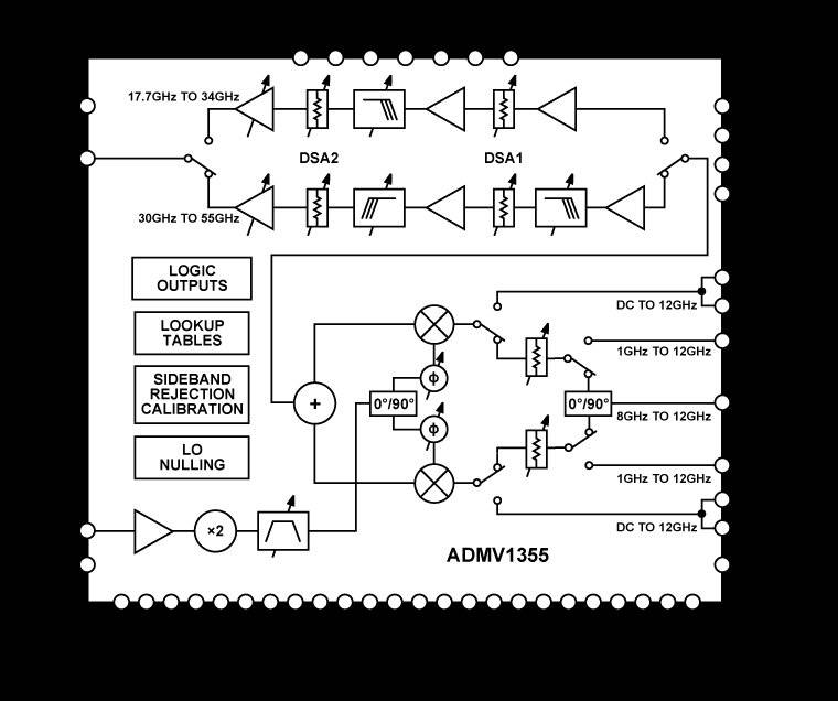
The device supports three frequency conversion modes, allowing different input configurations. In IF hybrid mode, a single IF input in the 8 GHz to 12 GHz range is processed through an on-chip 90° hybrid network to generate quadrature signals. In complex IF mode, two quadrature IF signals from 1 GHz to 12 GHz are used. In baseband mode, differential I/Q signals from DC to 12 GHz are accepted.
Programmability is achieved via a serial peripheral interface (SPI), supporting both 3-wire and 4-wire configurations. This interface enables adjustment of gain control, sideband suppression, LO carrier feedthrough calibration, and tunable filters. The device also includes general-purpose logic outputs and lookup table (LUT) inputs, suitable for system integration requiring fast frequency hopping.
All RF output, LO input, and IF input pins are single-ended and matched to 50 ohms, while the differential baseband I/Q inputs are matched to 100 ohms, eliminating the need for external matching circuitry.
The device is housed in a 120-ball CSP BGA package measuring 6 mm × 6.5 mm, operates over a temperature range of -40°C to +95°C, and supports heat dissipation through the package top or the printed circuit board.
Target applications include satellite payloads and ground stations, broadband radar and electronic warfare systems, instrumentation and automatic test equipment, as well as millimeter-wave 5G and 6G test platforms.
This article is compiled by Wedoany. All AI citations must indicate the source as "Wedoany". If there is any infringement or other issues, please notify us promptly, and we will modify or delete it accordingly. Email: news@wedoany.com