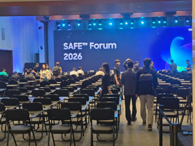
en.Wedoany.com Reported - At the SAFE Forum 2026 held at the Seoul Seocho office building, Samsung Electronics on the 1st unveiled its roadmap for the next-generation 2nm (nanometer, one-billionth of a meter) process, Design-Technology Co-Optimization (DTCO) technology, and high-performance SRAM. The company plans to collaborate with the Korean government's "Manufacturing AI Transformation (M.AX) Alliance" to develop on-device artificial intelligence (AI) chips, strengthening its role as a domestic system semiconductor platform.
Shin Jong-shin, Head of the Design Platform (DP) Development Office at Samsung Electronics' Foundry Business, stated in a keynote speech that Samsung will enhance its capabilities to meet AI demand, strengthen communication with customers and partners through the SAFE Forum, and formally initiate customer collaboration. This goes beyond foundry production to reinforce the company's role as a platform for Korea's domestic system semiconductor industry.
Park Sung-hyun, CEO of Korean AI fabless company Rebellions, introduced that the company has developed the "Rebel100" Neural Processing Unit (NPU) based on Samsung Electronics' 4nm foundry process and advanced packaging. He stated that collaboration in the AI semiconductor sector will continue to build sovereign AI. Jean Marie Brunet, Senior Vice President at global Electronic Design Automation (EDA) company Siemens EDA, also presented support solutions for rapidly implementing AI and High-Performance Computing (HPC) semiconductors using Samsung's advanced processes.
In addition to ecosystem collaboration, Samsung Electronics unveiled a customized process roadmap to address AI semiconductor demand. This includes DTCO technology for simultaneous optimization of design and process technologies, next-generation 2nm process technology, and plans to enhance the competitiveness of high-performance SRAM, aiming to improve Power, Performance, and Area (PPA) competitiveness. The company is working with the Korean government and academia to accelerate the expansion of the domestic system semiconductor ecosystem infrastructure. It is participating in the M.AX Alliance promoted by the Ministry of Trade, Industry and Energy to advance the development of low-power, high-performance on-device AI semiconductors for automotive, home appliances, robotics, and defense applications. Simultaneously, Samsung Electronics continues to support the Multi-Project Wafer (MPW) program, which reduces the initial prototype burden for domestic fabless companies, and participates in the "K-CHIPS" talent development program for master's and doctoral-level students.
The forum, themed "The Connection Point of Silicon Intelligence," attracted over 400 participants from global customers and partner companies. Twenty-one partners in the fields of Electronic Design Automation (EDA), Design Intellectual Property (IP), Design Service Platforms (DSP), Virtual Design (VDP), and Advanced Packaging (MDI) showcased solutions at exhibition booths. A Samsung Electronics official stated that as the AI semiconductor market expands, advanced process technology and ecosystem building capabilities have become core competitive advantages. To foster the development of the domestic system semiconductor ecosystem and enhance foundry competitiveness, Samsung Electronics will continue to collaborate with customers, partners, and the government, focusing on the SAFE and MPW programs.