en.Wedoany.com Reported - Samsung SDS, the information technology subsidiary of Samsung, is developing a technology that integrates quantum computing with artificial intelligence (AI) to simulate and improve the lithography process in semiconductor manufacturing. The company plans to test the technology through a proof of concept (PoC) in the second half of 2026. If successful, the system could be provided to Samsung Electronics for its semiconductor business.
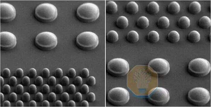
The lithography process uses light to transfer tiny circuit patterns onto silicon wafers, and its precision directly affects chip transistor density and production yield. Advanced chip manufacturing relies on precision step-and-scan lithography machines produced by Dutch equipment supplier ASML, which project designs onto a photosensitive layer on the wafer through a mask.
The core of the project lies in developing algorithms to virtually simulate the entire process before physical lithography. Quantum computers handle the main computations during the simulation phase, traditional computers process the generated data, and artificial intelligence identifies and corrects potential pattern errors. It is reported that Samsung SDS has already obtained some of the required algorithms and will test their effectiveness in a semiconductor manufacturing environment during the PoC phase. This system would enable Samsung to conduct virtual testing of circuit patterns before entering the high-cost physical production stage.
Accurate simulation helps detect lithography issues earlier, reduces the number of physical tests required to develop new manufacturing processes, and lowers the time and cost of patterning and etching wafers. By identifying defects before production, it is expected to increase the number of usable chips per wafer (yield). More precise patterning may also allow the company to place more transistors in a smaller area, enhancing chip density. Samsung anticipates that the combination of quantum computing, traditional computing, and AI correction will support the development of more advanced semiconductor processes.
Artificial intelligence has previously been used to improve computational lithography. Samsung has stated that by using Nvidia's cuLitho platform and CUDA-X libraries for optical proximity correction (OPC), its computational lithography performance improved by 20 times. Optical proximity correction predicts and adjusts pattern deviations that may occur when circuit designs are transferred to the wafer. The latest project extends this approach by incorporating quantum computing into the simulation process, but the technology is still under development, and its effectiveness depends on the results of the planned PoC.