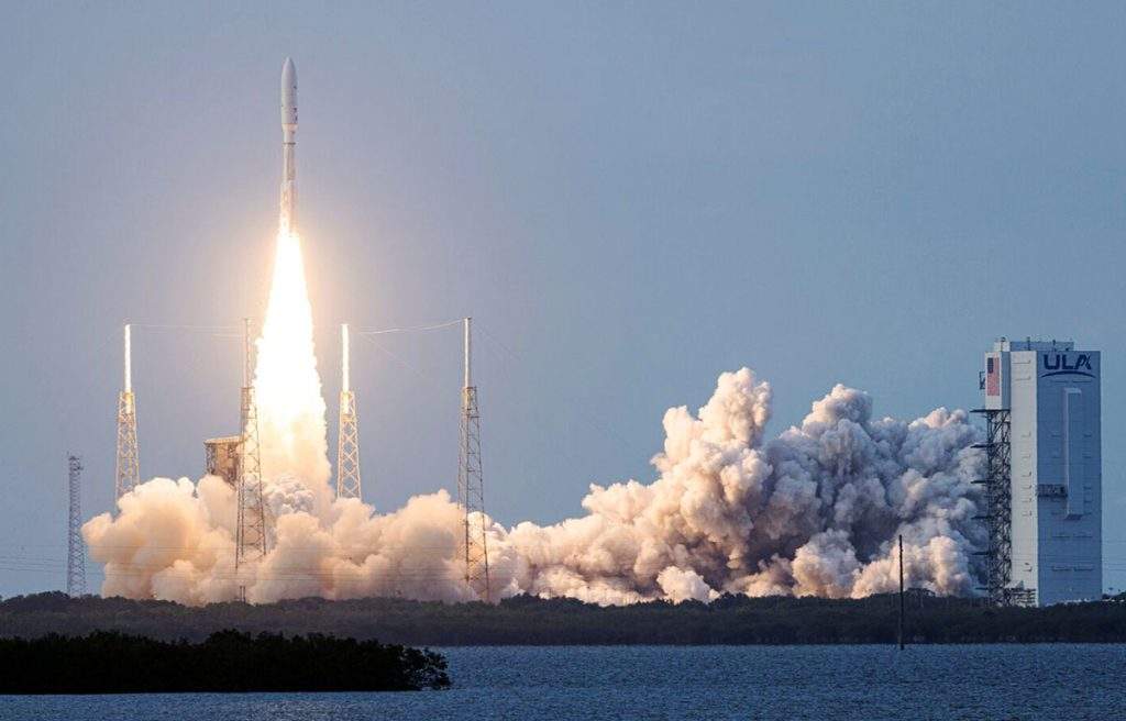
en.Wedoany.com Reported - As transistor density scaling slows, advanced packaging has become a primary scaling path. However, AI accelerators are large and require extremely high interconnect speeds, pushing packaging itself to its limits. Reticle interposers limit package size and wafer utilization, HBM4E technology doubles I/O count while increasing speed, and multi-kilowatt packages strain traditional cooling architectures.
ECTC is the industry's premier packaging technology event. This year's announcements are closely tied to upcoming commercial products. Intel outlined EMIB-T integration, package size scaling, and future roadmaps. Marvell demonstrated how custom HBM can move interface logic off the accelerator while shortening package routing. TSMC and Microsoft integrated coolant directly into silicon, while Marvell and Lightmatter integrated optical interconnects into packages.
This overview covers the technologies from ECTC 2026 most likely to shape AI accelerator solutions in the coming years.
Intel EMIB-T
Intel was the largest corporate presenter at ECTC. Its key showcase was EMIB-T, the next-generation EMIB chip using Through-Silicon Via (TSV) technology. Since the initial announcement, Intel has refined the architecture and roadmap, including smaller bump pitches, larger package sizes, and bridging capabilities. Their presentation indicated that EMIB-T is expected to be used in Google's TPU v9 and is the most viable alternative to TSMC's CoWoS platform in the large-package AI accelerator space.
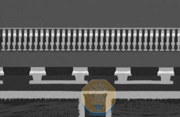
EMIB-T test chip, silicon content is twice the reticle size. Top-down SEM images show bump pitches of 110, 55, and 36 microns.
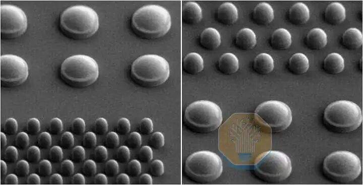
Intel has validated EMIB-T technology on chips packaged with double reticle-size silicon, achieving a bump pitch of 36/35 microns. This represents a 65% increase in bump density compared to the 45-micron pitch used in Granite Rapids packaging. Granite Rapids-AP is a large package measuring 70 mm × 105 mm, slightly less than 9 reticles. Validation for the 36/35 micron bump pitch is now being extended to 4.5x reticle-size silicon packages, targeting certification by the end of 2026.
The next pitch step is also underway, with Intel testing a 25 µm bump pitch based on a chip connecting two 1-reticle silicon chips via a single 3 mm × 18 mm EMIB-T bridge.
Further scaling will become more difficult. Below 25 µm, the solder volume in each ball becomes very small. The likelihood of shorts, opens, and yield loss during assembly increases significantly. EMIB-T can continue to scale, but the limiting factor shifts from bridge wiring density to solder ball formation, placement accuracy, and assembly yield.
Intel also demonstrated the size limits of EMIB-T packages. While full-panel-sized packages are possible, Intel targets quarter-panel packages as a practical goal. They showed a 240 mm × 240 mm test sample, an area roughly equivalent to 67 photomasks. However, the sample on display showed significant warpage. At this size, bridging is only part of the problem. Substrate handling, warpage, overlay accuracy, and panel-level patterning become primary limiting factors. Intel is also evaluating advanced lithography to ensure sufficient overlay accuracy for these large substrates at quarter-panel or even full-panel sizes.
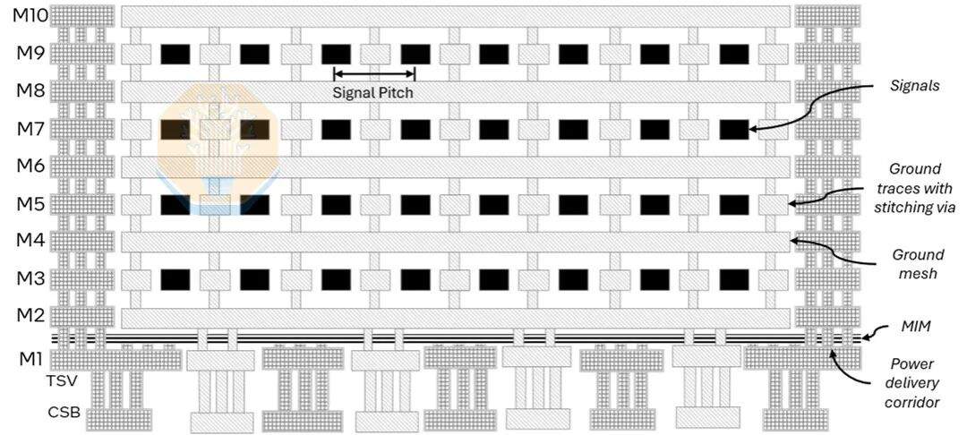
While bump pitch and package size are important, the bridge circuitry is equally critical. EMIB-T is significantly more complex than the EMIB used in current products. It adds TSVs, more metal layers, power grids, and MIM capacitor layers, enabling the bridge to simultaneously carry high-density signals and vertical power delivery. Intel showed a cross-section with 10 metal layers (including 4 routing layers) and MIM capacitors between M1 and M2. Intel highlighted its improvements for HBM4E.
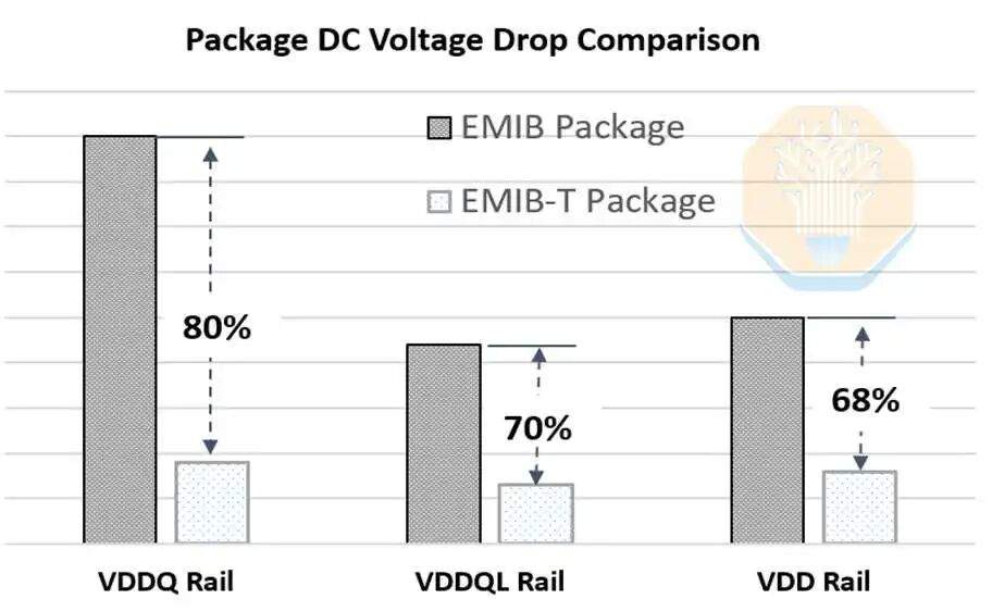
The "T" in EMIB-T stands for TSV (Through-Silicon Via). Their role is power delivery. In traditional EMIB, power in non-bridge areas is delivered vertically through the substrate, while power near the bridge area must spread laterally into package and chip-side wiring. By using TSVs in the bridge area, power can be delivered directly through the bridge, significantly shortening the current path. Intel claims using these TSVs can reduce DC voltage drop by 68% to 80%.
The challenge for HBM4E is that interconnects must simultaneously increase signal density and power delivery capability. HBM4 has twice the pin count of HBM3, and the PHY requires additional power rails like VDDQ and VDDQL. These power rails consume some signal routing space, thereby increasing signal density in the remaining space.
To address this, Intel does not route all HBM channels identically. It places the longest signal paths on layers with cleaner routing. On the M9 layer, only about 28% of the longest channel length passes through the most densely routed area, while on lower layers like M3, this percentage rises to about 84%, but these channels are shorter. This prevents crosstalk and insertion loss from being dominated by the worst-routed areas.
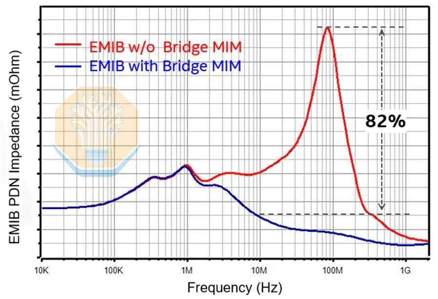
Power delivery is also moved to the bridge layer. EMIB-M introduced Metal-Insulator-Metal (MIM) capacitors between M1 and M2, and EMIB-T improves upon this. Intel reported a capacitance density of 500 nF/mm², roughly comparable to Intel 18A's MIM capacitors. Intel claims these bridge capacitors can reduce the AC impedance of the Power Delivery Network (PDN) by over 82% compared to an EMIB-T package without bridge MIM capacitors.
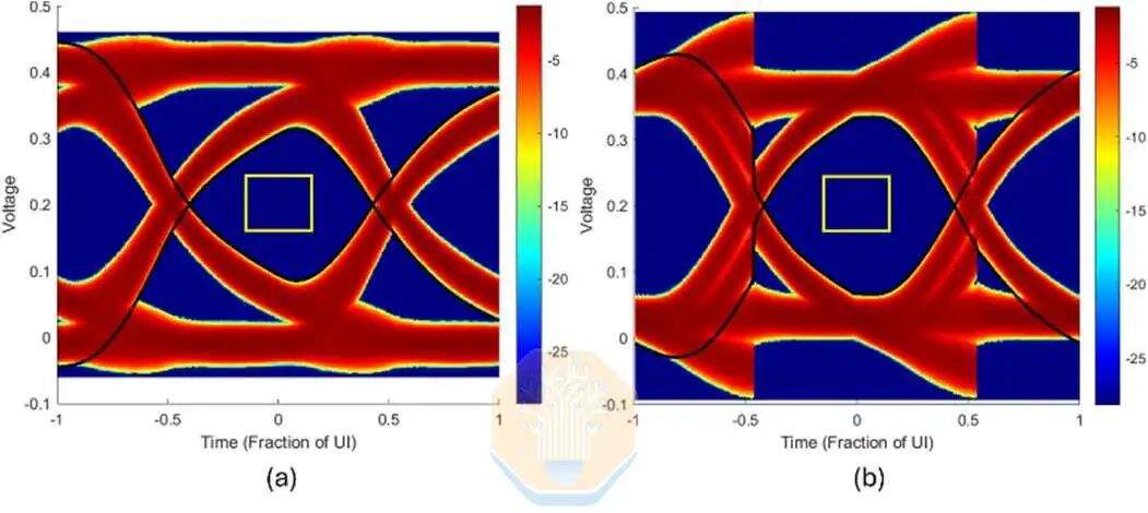
Intel also performed simulations for EMIB-T with HBM4E. At 12 Gb/s, without receive equalization, Intel's UI eye width was approximately 67%. Using a single-tap Decision Feedback Equalizer (DFE), this improved to about 72.5%. DFE is a receiver circuit that reduces interference from previous bits after the signal passes through the package channel.
Intel also simulated higher data rates: 12.8 Gb/s, 14 Gb/s, and 16 Gb/s. At all tested speeds, the UI eye width remained above 60%, with a slight decrease in pad capacitance.
Intel's EMIB roadmap extends beyond passive bridges containing only wiring and capacitors. Future versions will include higher density bridge MIM capacitors, larger high-aspect-ratio bridge chips, sub-25 micron bump pitches, active bridges, and voltage regulators integrated within the EMIB chip. Intel also disclosed concepts for substrate core embedded Deep Trench Capacitors (DTC) and >2500 nF/mm² eMIM-T capacitors embedded beneath the substrate, although these have not yet been seen in shipped EMIB products.
EMIB-T still lags behind TSMC's CoWoS platform in several areas. TSMC has achieved DTC/eDTC integration and is further along with integrated voltage regulators and active Local Silicon Interconnects (LSI). EMIB-T closes the gap, but Intel is still catching up to an ecosystem that has been running at scale for years.
Marvell Custom HBM
At Marvell's 2024 Industry Analyst Day, Marvell announced Custom HBM. At the time, it was a vague statement lacking technical details. HBM design has always revolved around JEDEC compatibility: standard DRAM stacks from memory vendors, standard HBM PHYs on accelerators, and a fixed wide interface between them. At Hot Chips 2025, Marvell showed a layout of the custom base die.
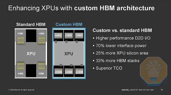
At ECTC, Marvell finally provided package-level details for Custom HBM4E.
The JEDEC specification fixes the interface between the HBM stack and the host. This benefits interoperability: any memory vendor's HBM can pair with any compatible host. However, it hurts power, performance, and area. The host ASIC must implement a standard HBM PHY with standardized pad layouts and breakout rules, routing a very wide parallel interface. As package sizes increase and HBM speeds rise, this fixed boundary makes optimizing coastline, routing density, power delivery, and signal integrity more difficult.
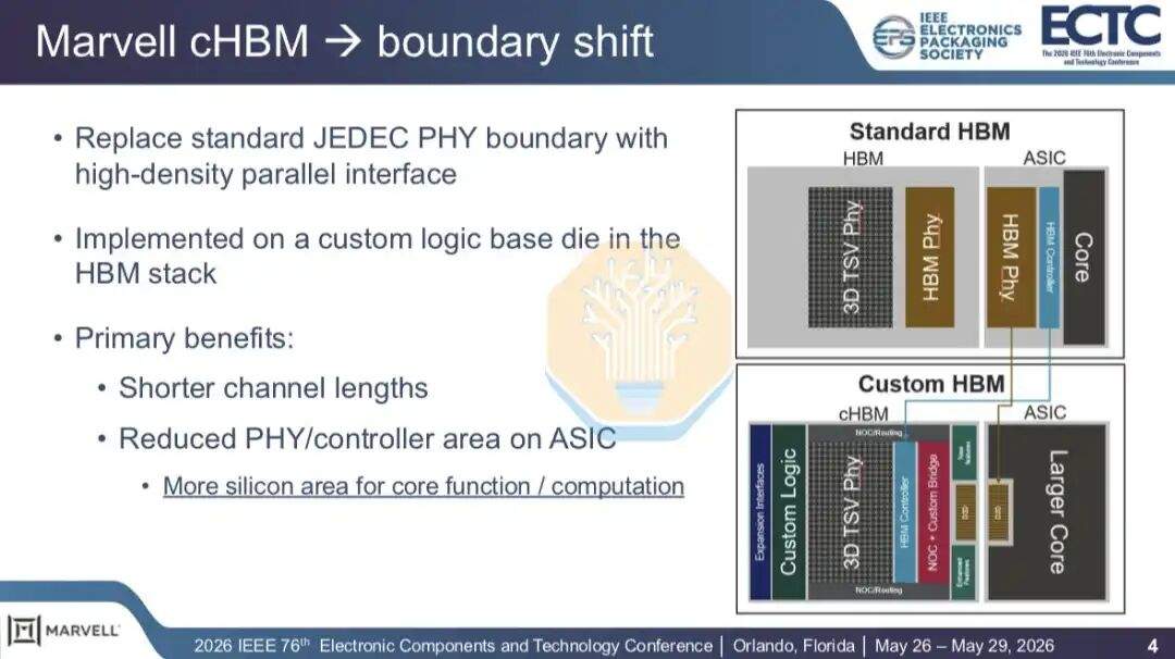
Custom HBM technology requires no changes to the DRAM core chips. Instead, a custom base die is manufactured using an advanced logic process with an optimized die-to-die interface. This custom base die can integrate the HBM controller, management and monitoring functions, custom logic, and an extended interface.
Marvell claims this reduces the host ASIC footprint for the HBM PHY and related logic by approximately 60%, directly freeing up more space for compute, cache, or I/O. This custom interface moves most of the memory-side interface into the HBM base die.
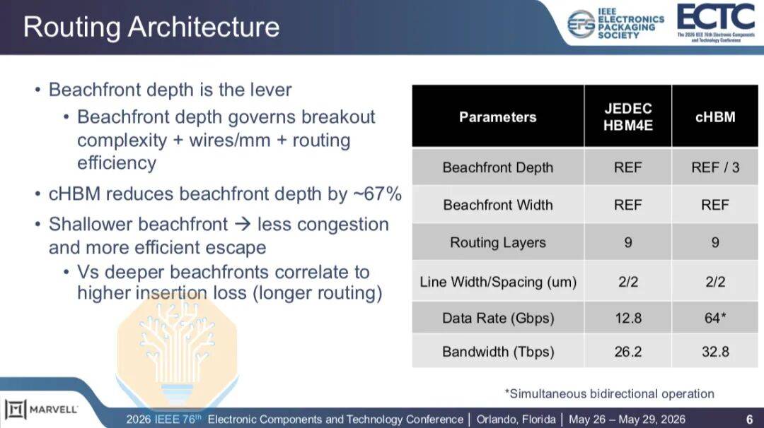
Marvell's example uses 1024 channels at 32 Gb/s, achieving 4.1 TB/s, equivalent to a 2048-bit JEDEC HBM4(E) interface at 16 Gb/s.
Package routing also becomes easier, with the custom interface reducing interposer channel length from 6.5 mm to 1.5 mm, allowing Marvell to increase bandwidth while maintaining the same 9 routing layers and 2/2 micron line/space (L/S).
Marvell's example uses an organic Redistribution Layer (RDL) interposer instead of silicon, reducing package cost. Organic RDL has much larger line/space than silicon interposers in CoWoS-S or silicon bridges in CoWoS-L and EMIB-T, increasing routing difficulty. Marvell relies on custom shielding and routing patterns in different sections to maximize bandwidth density while controlling crosstalk.
At GTC, Nvidia announced that Feynman will use Custom HBM. Nvidia's rationale is likely similar to Marvell's: higher bandwidth, lower power, and less HBM accelerator chip area. Approximately 16% of the Rubin GPU chip area is dedicated to HBM-related logic and PHY. Custom HBM allows Nvidia to shift most of this burden to the HBM base die.
Custom HBM also supports extended interfaces beyond standard HBM links. The base die can act as a secondary memory controller and fan out traffic to additional memory, rather than forcing all memory traffic through the limited accelerator chip edge channels. This additional memory could be higher-capacity, lower-bandwidth LPDDR, or even a second tier of HBM. This allows accelerators to scale memory capacity without consuming precious chip edge channels needed for external I/O. This is particularly important for AMD's upcoming MI450 and future MI500 GPUs, which will support LPDDR for increased memory capacity.
Samsung HBM Interposer
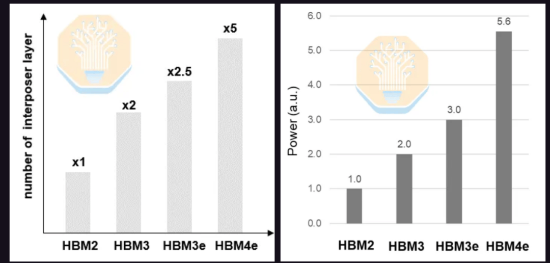
Samsung also showcased its interposer-based HBM4E solution. HBM4E increases data rates to 12 Gb/s and beyond and doubles the number of I/O pins, increasing routing complexity. The number of interposer layers required for HBM4E could be double that of HBM3E and five times that of HBM2. Due to the increased I/O pin count and higher data rates, power consumption is also expected to increase by 86% compared to HBM3E and 5.6 times compared to HBM2.
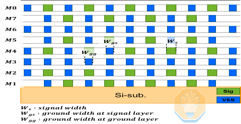
Samsung proposed an 8-layer silicon interposer solution, claiming a 20% reduction in layers compared to estimated requirements. The interposer uses a repeating dual-signal/single-ground interleaving pattern to shield high-speed signals, with 75% of the layers dedicated to signal routing.
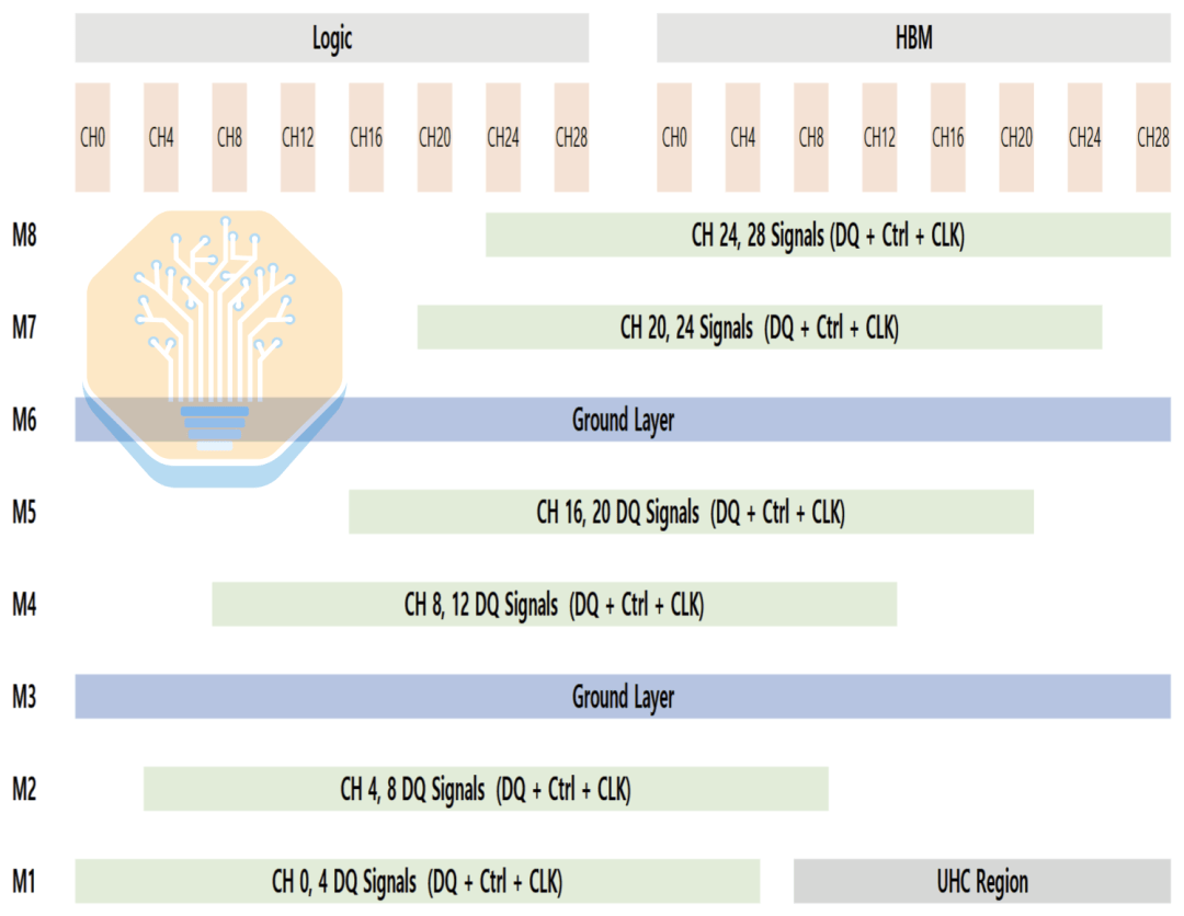
Another key feature of the interposer is the Ultra-High Density Capacitor (UHC). Samsung did not specify the exact capacitor structure, but they are likely similar to Intel's EMIB-T MIM capacitors or TSMC's CoWoS DTC capacitors. UHC capacitors can only be placed on the M1 layer, which is also primarily used for signal routing, limiting available area.
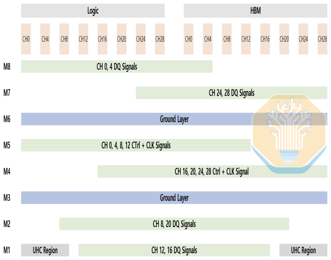
If routing is unbalanced, capacitors are pushed to one side of the interface, leading to uneven Power Delivery Network (PDN) performance between the logic side and the HBM side. Samsung's layout redistributes routing to the M1 layer and other layers, allowing the UHC to be distributed more evenly across the entire interface. This reduces PDN impedance and voltage noise while maintaining manageable routing density.
Samsung HBM Hybrid Bonding Thermal
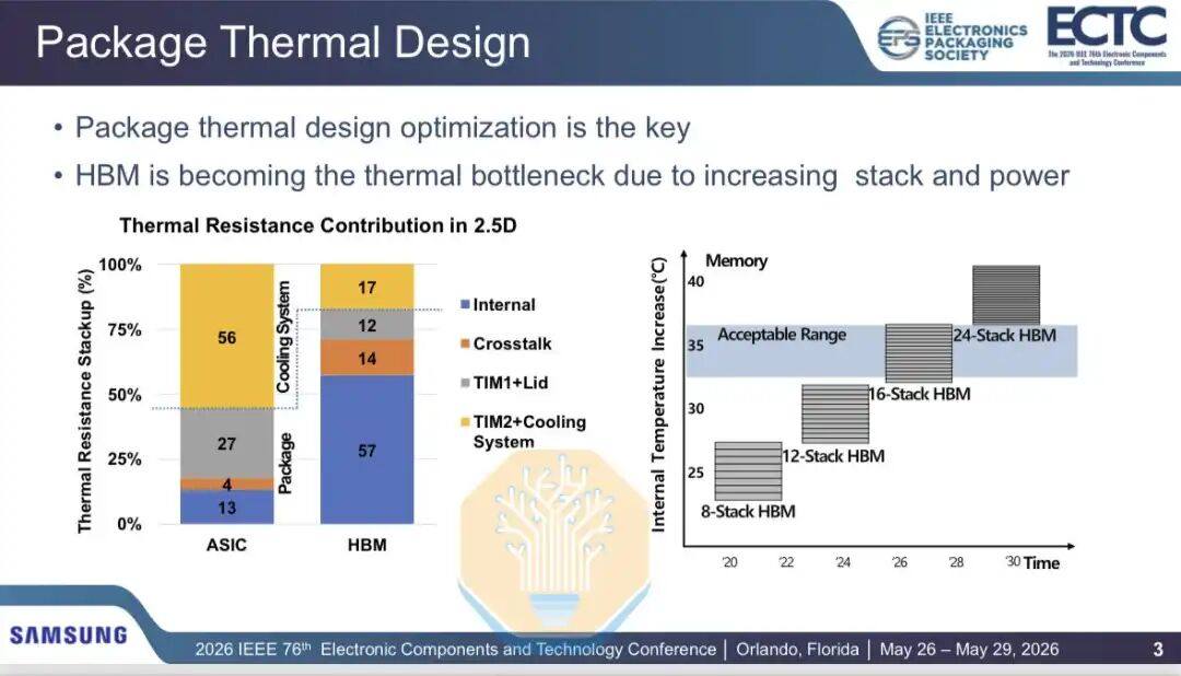
Samsung also discussed thermal issues in HBM, specifically regarding hybrid bonding. HBM stacks are getting taller and faster, while the logic chips beneath them are consuming more power. For 16-layer HBM, thermal resistance is acceptable, but as future generations move to 20-layer and 24-layer HBM, new solutions are needed.
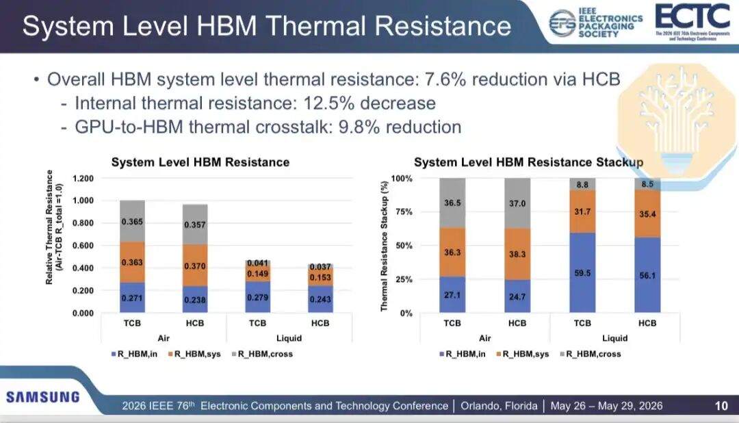
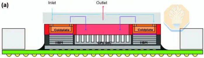
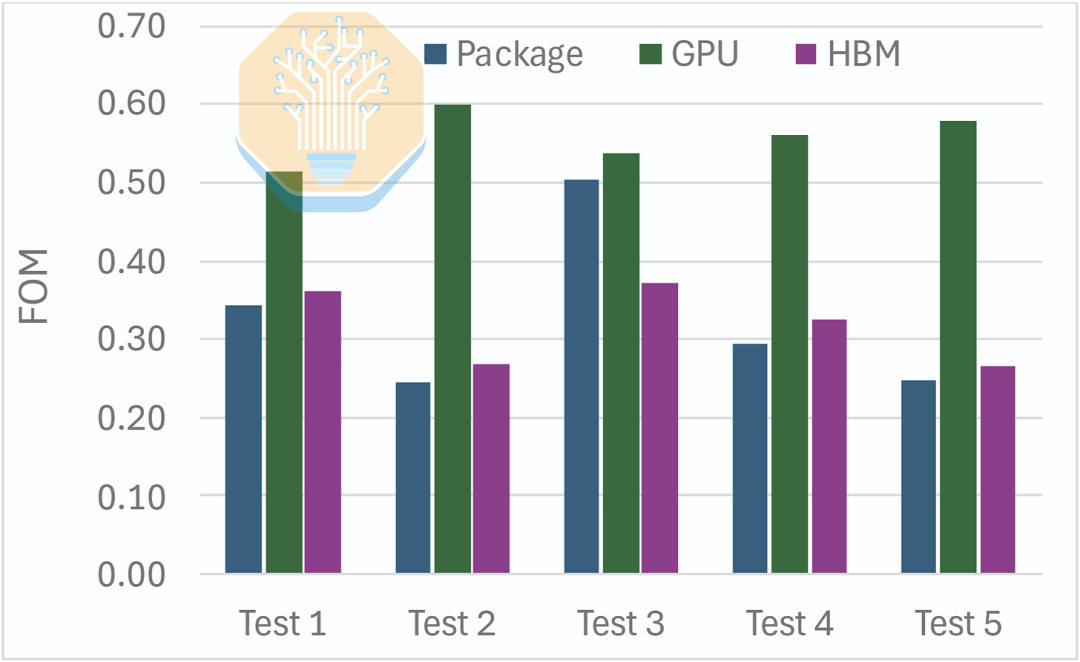
Samsung compared the thermal performance of Thermal Compression Bonding (TCB) and Hybrid Copper Bonding (HCB) for HBM in a 2.5D GPU package (containing 2 GPU chips and 8 HBM stacks, similar to the Nvidia Blackwell architecture). Results showed that air cooling reduced internal HBM thermal resistance by 12.2%, and liquid cooling reduced it by 12.9%. Total HBM thermal resistance was reduced by 3.5% with air cooling and 7.7% with liquid cooling.
Because HCB only targets part of the thermal network, the improvement is not uniform. Samsung divided the thermal path into internal resistance, system-level resistance, and GPU-to-HBM crosstalk. Internal resistance and crosstalk decreased by approximately 12.5% and 9.8%, respectively, but system-level resistance, including thermal interface material and heatsink, increased by about 2.3%.
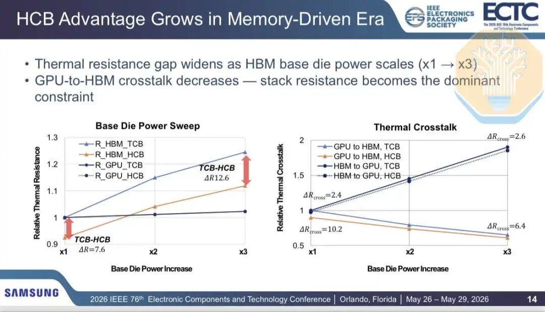
As more power shifts to the HBM base die (e.g., in memory-intensive workloads), the thermal bottleneck shifts. This is particularly important for Custom HBM, where the memory controller and more logic are integrated into the base die. GPU-to-HBM crosstalk becomes a smaller portion of total thermal resistance, dropping from 13% with a 1x increase in base die power to 5% with a 3x increase.
Samsung stated that using HCB technology allows for higher inlet temperatures or increased package power. It estimates that with HCB, inlet temperature can be increased by 1-2°C while maintaining package power, or package power can be increased by approximately 4% while maintaining temperature. Samsung also estimates a reduction in thermal design power of about 7%.
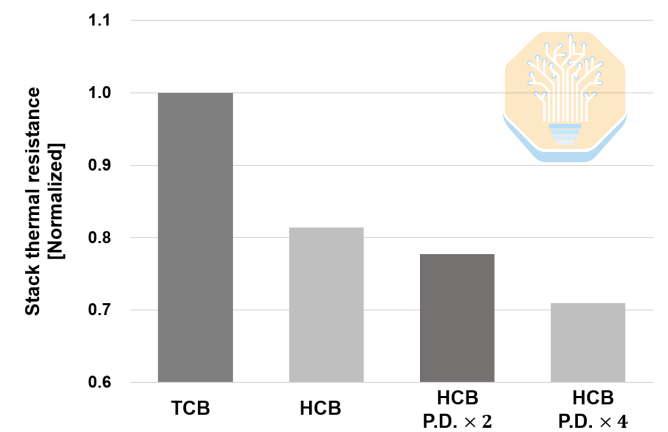
Samsung also studied the impact of HCB at the stack level separately. The improvements here are larger: baseline HCB reduces stack thermal resistance by approximately 19% compared to TCB. Increasing the number of HCB pads, with a 2x increase in pad density, yields a thermal resistance reduction of up to 22.3%; a 4x increase yields up to 29.1%.
Microfluidic Cooling
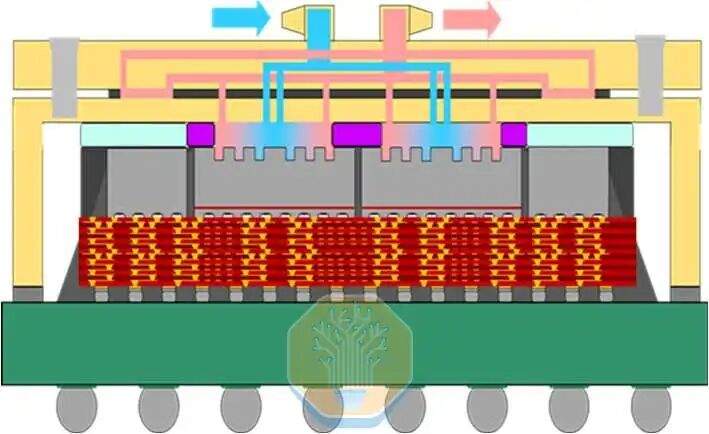
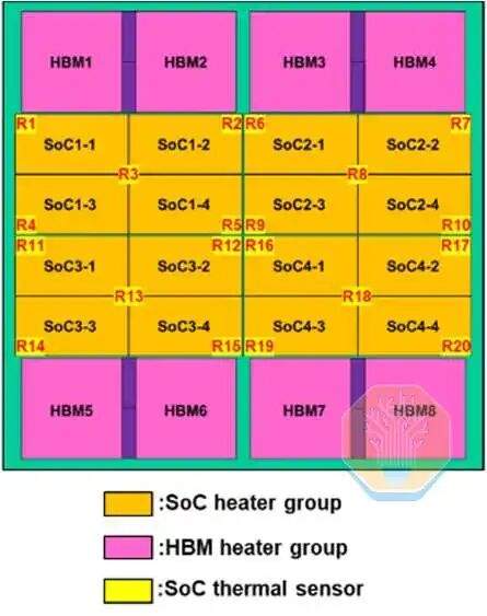
TSMC demonstrated direct silicon cooling on a CoWoS-R chip, used in a large GPU-like test vehicle. CoWoS-R differs from CoWoS-S in using organic materials instead of a silicon interposer. CoWoS-R was chosen for its better warpage tolerance and process compatibility. The test vehicle uses a 3.3x reticle interposer containing 4 SoC chips and 8 HBM stacks. Each SoC chip consists of 4 groups of SoC heaters, collectively covering approximately half the interposer area.
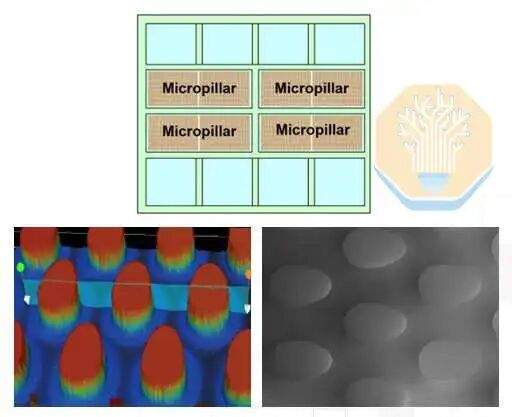
TSMC compared three solutions: a traditional package with a lidded cold plate, a lidless cold plate package, and its micro-pillar direct silicon package design. The lidded and lidless solutions still use traditional cold plates and Thermal Interface Material (TIM). The final solution forms micro-pillars directly on the backside of the SoC chip.
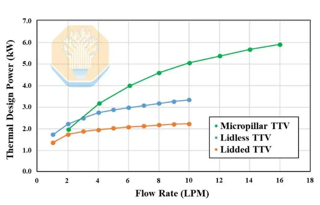
With conventional cooling at a flow rate of 1-2 liters per minute (LPM), the lidded package dissipated 1.9-2.3 kW, while the lidless package dissipated 2.5-3.0 kW, using deionized water at 40 °C. Both solutions saturated after flow rates exceeded 4 LPM, as the TIM became the bottleneck.
The micro-pillar test vehicle performed comparably to the lidless cold plate at 2 LPM, then outperformed it at higher flow rates, dissipating 4 kW at 4 LPM and 5.3 kW at 8 LPM. TSMC reported uniform heat dissipation exceeding 5 kW across the entire test vehicle. The micro-pillar structure brings the liquid coolant closer to the heat source, facilitating this performance improvement.
However, the micro-pillar structure is not without challenges. TSMC had to form the micro-pillars after the Chip-On-Wafer (CoW) process, while avoiding damage to the CoWoS-R structure, and develop new sealing materials to ensure coolant containment despite package warpage and Coefficient of Thermal Expansion (CTE) mismatch. The test samples passed Moisture Sensitivity Level 4 (MSL4) testing without helium leakage or sealant delamination.
Microsoft's cooling solution differs from TSMC's in its cooling structure. TSMC uses silicon micro-pillars, while Microsoft uses straight microchannels etched into the GPU silicon. Instead of a thermal test vehicle, Microsoft tested directly on an Nvidia GH200 GPU. This likely allowed Microsoft to capture real thermal distributions and hot spots more accurately. Microsoft tested various workloads on the GPU, such as HPCG and HPL, each with different compute and memory stress characteristics.
Under these workloads, Microsoft reported a 51-60% reduction in GPU junction-to-inlet thermal resistance at a flow rate of 1 LPM. The improvement for HBM was smaller, at 27-37%, as it is still cooled via a cold plate and thermal material. Overall, this resulted in a 50% reduction in package thermal resistance.
Microsoft also presented some preliminary reliability data. While thermal performance is important, data center deployment also requires high reliability and low downtime. Over a 6-month period, Microsoft recorded only 9 potential clogging events in approximately 4,370 observations. The clogging rate decreased over time, suggesting initial instability followed by a more stable operational phase. Even after 6 months, there was no measurable silicon corrosion in the microchannels. At the node level, the GH200 successfully completed 3 weeks of repeated benchmark testing, followed by 1 week of continuous operation at a stable package power. Microsoft is still testing Mean Time Between Failures (MTBF) and availability at the cluster level.