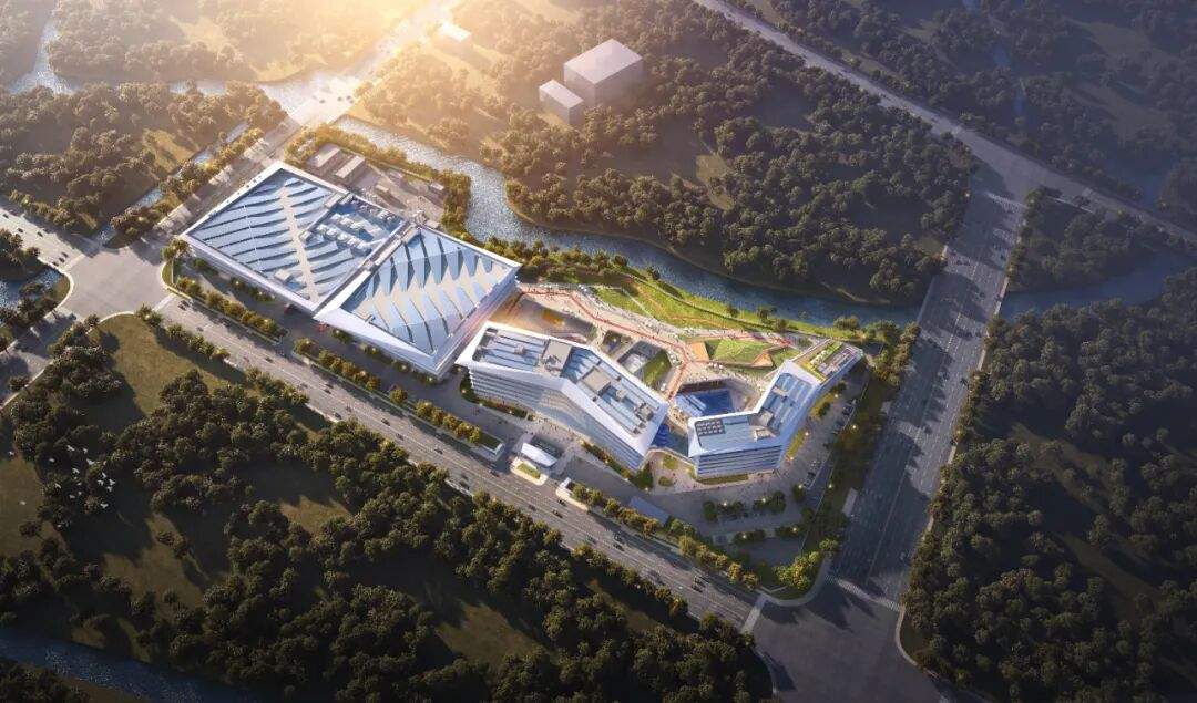
en.Wedoany.com Reported - On June 30, the Haining Economic Development Zone marked another significant milestone—the official launch of the Tuojing Jianke (Haining) Semiconductor Equipment Co., Ltd. project for the research, development, and industrialization of advanced semiconductor process equipment.
From its initial connection in 2020, to the signing of an upgraded agreement in 2024, and now the formal implementation of this second-phase project, Tuojing Jianke has completed a six-year journey from "strategic positioning" to "deep cultivation," signaling a new phase of deep, full-chain integration in government-enterprise cooperation.
"Six years ago, we evaluated multiple locations and ultimately chose Haining, drawn by the city's foresight and strategic commitment to the semiconductor industry," recalled Dr. Lyu Guangquan, Chairman of Tuojing Group. He noted with a smile that at the time, the "τ law" and wafer bonding technology were still unfamiliar to many, but Haining had already demonstrated the boldness to plan ahead.
Over the past six years, Tuojing Jianke has consistently focused on wafer bonding technology, a core process in three-dimensional integration, achieving a full-chain leap from team building and technical breakthroughs to product validation and mass production delivery. It became the first company in China to achieve mass production of hybrid bonding equipment, establishing itself as a leader in the field.
"From R&D subsidies and land guarantees to talent housing and industrial collaboration, Haining has provided tangible support. This is the fundamental reason we dared to place our second-phase heavy assets here," said Lyu. The new project will strongly support the company's scaled development while injecting new momentum into Haining's semiconductor equipment industry chain, reinforcing and upgrading it.

The project is being constructed by Zhejiang Jinghua Construction Co., Ltd. Chairman Xu Mingliang stated that this project represents a new high ground for innovation and manufacturing of domestic semiconductor equipment, requiring high construction precision, and the company will go all out to ensure high-quality progress.

The Haining Economic Development Zone will provide proactive, full-process services and precise support to ensure the project's smooth progress, aiming for early completion, early production, and early results. At the same time, it will continue to optimize the industrial ecosystem, leveraging chain-leading enterprises like Tuojing Jianke for targeted investment attraction, drawing more upstream and downstream industry chain companies to accelerate clustering, and jointly enhancing Haining's reputation in semiconductor equipment manufacturing.