Samsung and SK Hynix Delay Adoption of Hybrid Bonding Technology for HBM
en.Wedoany.com Reported - Samsung Electronics and SK Hynix are reassessing their plans to introduce hybrid bonding technology in next-generation High Bandwidth Memory (HBM), as the necessity of its two core advantages—reduced thickness and enhanced heat dissipation—is diminishing.
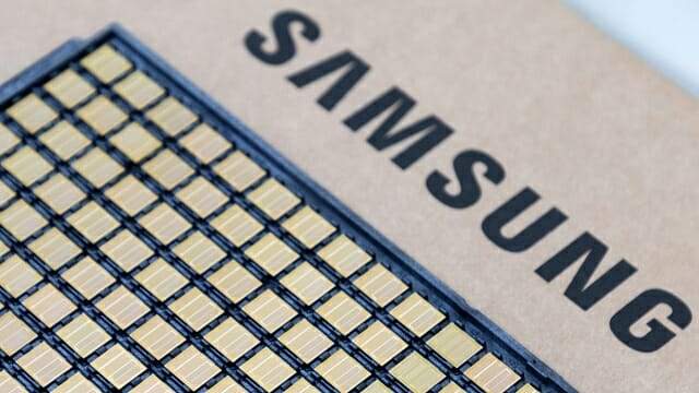
According to industry sources, the full-scale adoption of hybrid bonding in next-generation HBM may occur later than expected. Earlier predictions suggested that the technology could be applied starting with HBM4 (the sixth generation of HBM), but this has not materialized due to high technical difficulty. Current forecasts indicate that hybrid bonding might be adopted from 16-layer HBM4E (the seventh generation of HBM), pushing back the expected timeline. Currently, Samsung Electronics and SK Hynix continue to use Thermal Compression (TC) Bonding in mass production, which involves adding micro bumps and underfill material between DRAM layers and connecting them through heat and pressure.
Hybrid bonding technology directly connects the copper wiring of each DRAM layer, eliminating the need for bumps and underfill material, thereby reducing the overall thickness of HBM and improving heat dissipation characteristics and power efficiency. However, industry experts point out that the two main drivers for adopting hybrid bonding are weakening. On one hand, HBM thickness standards are being relaxed: the thickness standard for HBM3E is 720 micrometers, while for HBM4 it has been raised to 775 micrometers, due to the increase in DRAM stacking layers from 8 or 12 layers to 12 or 16 layers. The International Semiconductor Standardization Organization (JEDEC) is even considering relaxing the thickness standard for next-generation HBM with 20 stacked layers (such as HBM5) from 900 micrometers to around 1000 micrometers. On the other hand, demand from key customers like NVIDIA for HBM with high stacking layers has been delayed. A memory manufacturer source noted that discussions on 16-layer HBM have not yet been actively conducted with customers, and 12-layer HBM4E products are likely to remain the mainstream.
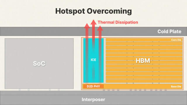
To compensate for the heat dissipation advantages of hybrid bonding, Samsung Electronics and SK Hynix are exploring alternative solutions. Samsung Electronics has proposed the Heat Path Block (HPB), while SK Hynix has introduced the iHBM (ICE HBM) concept. Both involve placing a dedicated heat-dissipating component next to the core HBM chip. Packaging industry insiders say that this technology is not difficult to implement and arrange, has clear commercialization prospects, and represents a stable option for memory companies. Both companies are testing the application of this technology to HBM5.
Although the adoption of hybrid bonding may be delayed, Samsung Electronics and SK Hynix continue their research and development of the technology. In the long term, the increase in the number and density of internal I/O (input/output terminals) in HBM will make hybrid bonding technology necessary. The number of I/Os in HBM4 has already doubled compared to the previous generation HBM3E, reaching 2048. TC bonding, due to the lateral diffusion of melted bumps, struggles to support further increases in I/O density. Packaging industry experts point out that if the number of I/Os in HBM5E doubles again to 4096, the I/O pitch will become extremely narrow, making the adoption of hybrid bonding technology imperative.
Related Products



G.652.D Wavelength-extended Non-dispersion Shifted Single-mode Optical Fiber
HONGAN GROUP CO., LTD.

Multi-function Marine Monitoring Low-altitude Detection Radar Sea-air Boundary Ocean Dynamic Environment Measurement
Chengdu Dixin Technology Co., Ltd.
20 Inch 1600*900 Full HD 60Hz TFT LED Monitor with VGA and DP Interfaces for Desktop Computers-Business Use
Guangzhou Zanying Optoelectronics Technology Co., Ltd.
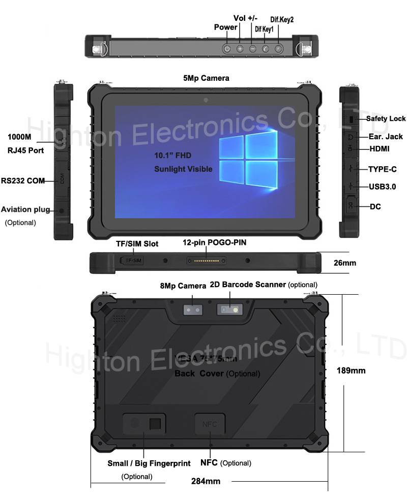
Hot Selling 10 Inch Intel N5100 I5 I7 FHD 8 +128GB 16+256GB Win10 Pro Win11 Pro 4G 5G Rugged Tablet PC Pad with NFC Barcode
Highton Electronics Co., Ltd.
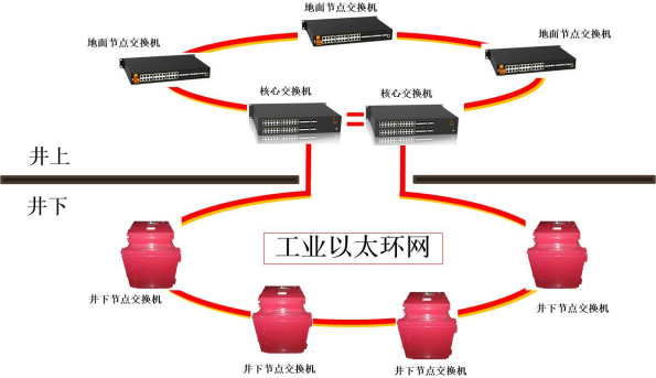
Mine Explosion-proof and Intrinsically Safe Industrial Ethernet Ring Network (10 Gigabit/Gigabit)
Chongqing Mas Sci&Tech Co., Ltd.
GYTA Type Non-Self-Supporting Aerial/Duct Optical Cable
TONGDING INTERCONNECTION INFORMATION CO., LTD.