ZEISS Opens World's First Semiconductor Innovation Center in South Korea
en.Wedoany.com Reported - ZEISS has opened its first global semiconductor innovation center in Yongin, Gyeonggi Province, South Korea, to strengthen local responsiveness for next-generation semiconductor solutions such as High Bandwidth Memory (HBM) and 3D memory, accelerating development processes.
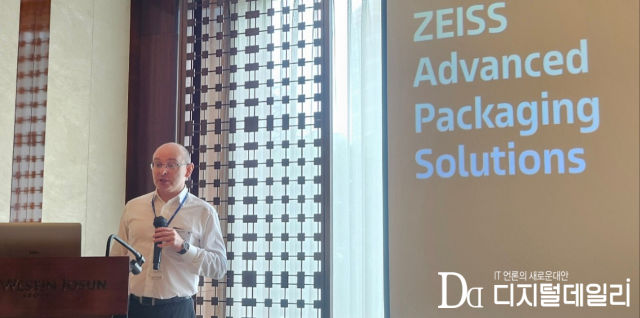
ZEISS held a press conference in Seoul on the 10th, announcing the establishment of the "ZEISS Semiconductor Korea Innovation Center (ZSKIC)" within the SeoPlus global semiconductor equipment cluster in Yongin, Gyeonggi Province. Attendees included Matthew Wilson, Vice President of ZEISS Semiconductor Business Unit Korea; Caroline Pigdon, Head of Semiconductor Fab Solutions; and Michael Henschel, Head of Advanced Packaging Solutions.
As a global optical technology company headquartered in Germany, ZEISS' business spans consumer lenses for eyewear and cameras, as well as measurement and optical solutions for industrial and medical fields. In the semiconductor sector, it supplies lenses for ASML's Extreme Ultraviolet (EUV) lithography systems and provides solutions for photomask measurement and repair, wafer inspection and measurement, defect analysis, wafer shape control, and advanced packaging process control.
Spanning 350 square meters, ZSKIC is an on-site solution validation space for customer demonstrations, evaluations, and the production of customized solutions tailored to the mass production environment requirements of semiconductor chip manufacturers. This marks the first time ZEISS has established a global innovation center in a regional market, with South Korea being the first country to host it.
ZEISS plans to deploy core fab solution equipment from its semiconductor division to ZSKIC to accelerate customer delivery times. This means basic development and validation will be conducted at the center with local South Korean customers such as Samsung Electronics and SK Hynix. Once the technology matures, it will be transferred to the field, and new equipment will be introduced. Currently, two pieces of equipment have been prioritized for installation at the center, with a third to be introduced soon, allowing for a maximum of four operational units.
![Two pieces of equipment introduced at the Yongin ZEISS Semiconductor Innovation Center [Photo: ZEISS]](https://img.wedoany.com/2026/0711/20260711020538641.jpg)
With the recent increase in the importance of advanced packaging processes, ZEISS has prioritized the deployment of the 3D X-ray measurement equipment "NLX-100" and the wafer warpage control equipment "DUNE-100." Advanced packaging, a back-end semiconductor process, involves wiring connections or assembling external protective devices on wafers with circuit patterns. As circuit miniaturization faces physical limits, the frequency of vertical chip stacking or bonding has increased, making packaging a critical process determining chip performance and power efficiency.
Caroline Pigdon, Head of Fab Solutions, stated that ZEISS aims to improve customer yield and reduce defects by providing inspection, measurement, defect analysis, wafer shape control, and advanced packaging tools. The new tools primarily focus on the advanced packaging field, which presents many new process challenges.
The NLX-100 is an in-line 3D X-ray measurement and inspection device used to find defects in front-end and advanced packaging processes. In advanced packaging, it can non-destructively analyze micro-bump pitch defects connecting chips to substrates, as well as connection defects between Through-Silicon Vias (TSVs) and bumps, providing defect information to process development teams and operation engineers to help adjust process parameters.
The DUNE-100 is a system for controlling and correcting wafer warpage, which can be caused by factors such as metal layer deposition and heat, leading to focus errors or alignment issues in subsequent processes like exposure, bonding, and stacking. ZEISS states that the DUNE-100 can correct wafer warpage of up to 700µm and correct distortions in specific areas without requiring chemicals like Chemical Mechanical Planarization (CMP) slurry.
ZEISS's choice of South Korea for its first local innovation center stems from the speed of technological iteration driven by the proliferation of Artificial Intelligence (AI) infrastructure. With the development of AI, the development speed of semiconductor chips is accelerating. To respond to this trend, validation must occur in South Korea, which can supply AI infrastructure memory the fastest. The fact that major customers like Samsung Electronics and SK Hynix are expanding investments in memory, HBM, and advanced packaging in South Korea has also been a significant factor.
Vice President Matthew Wilson emphasized that the AI super cycle is accelerating semiconductor development cycles. Without timely solutions, even world-class optical technology cannot fully play its role. South Korean customers need technology at the speed they desire, and the establishment of the center in South Korea aims to achieve this.
Vice President Wilson added that Yongin will become a new semiconductor hub in South Korea. The importance of the South Korean semiconductor ecosystem and the positive investment policies over the next decade form the backdrop for the center's establishment. As sending wafers or photomasks to overseas factories in Germany, Israel, and the United States for testing becomes increasingly difficult, the necessity of collaborating with local customers and accumulating expertise is growing.
The performance improvement of advanced packaging in the memory field has also been a driving force. Unlike the past focus on low-mix, high-volume production, the application methods of memory like HBM, 3D NAND and DRAM, and 3D logic packaging are diversifying. Therefore, validation must be prioritized in South Korea to respond quickly to process changes.
Michael Henschel, Head of Advanced Packaging Solutions, stated that advanced packaging is currently the most important topic in the industry and a core driver of the AI super cycle. The NLX-100 and DUNE-100 are equipment customers need to enter mass production.
Henschel particularly emphasized the potential applications of the DUNE-100, a new concept system introduced by ZEISS for the first time. Currently, the equipment supports 3D NAND, 3D logic, CMOS, and 3D DRAM. The main application scenarios developed with customers are in the pre-bonding and lithography process stages. If wafer warpage occurs, focus issues may arise before and after lithography, and the DUNE-100 helps correct this problem.
Regarding the application of the X-ray measurement system NLX-100, Henschel explained that considering support for HBM production, reducing X-ray dose is an important roadmap item. In the long term, its use for hybrid bonding (operating two dies as a single unit) is also being considered. During hybrid bonding, the spacing between chips and between chips and substrates decreases, requiring further improvement in the NLX-100's resolution, which is also a challenge.
Henschel emphasized that customers highly value ZEISS's excellent image quality and dose control for protecting chips like HBM. ZEISS considered dose limitations and protection concepts from the early design stage. Furthermore, possessing complete technology from the light source to the entire beamline and software allows independent control over the roadmap's speed.
ZEISS plans to introduce the next-generation photomask repair equipment "MeRiT AE" to South Korea in the future and expand its response scope based on the outcomes of ZSKIC. The MeRiT AE is used to inspect fine defects within photomasks (master templates for drawing semiconductor circuits) and remove unnecessary patterns or defects. ZEISS plans to introduce the first prototype of the MeRiT AE to South Korea for collaboration with customers on next-generation processes like High-NA EUV.
Frank Romund, CEO of ZEISS Semiconductor Business Unit, stated that South Korea is a core hub of the global semiconductor industry. He expressed hope that through the establishment of this center, ZEISS can become a trusted long-term partner for South Korean customers and will continue to strengthen cooperation in the future.
Related Products

20 Inch 1600*900 Full HD 60Hz TFT LED Monitor with VGA and DP Interfaces for Desktop Computers-Business Use
Guangzhou Zanying Optoelectronics Technology Co., Ltd.
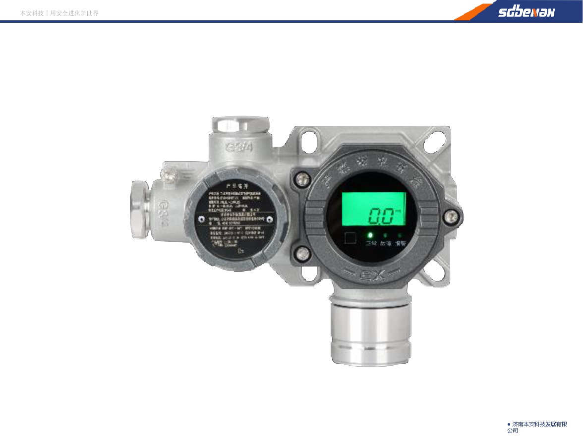
Industrial and Commercial Point-Type Gas Detector
Jinan Benan Technology Development Co., Ltd.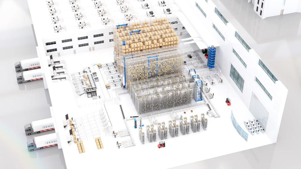
One-Stop Steward Service for the Entire Logistics System Integration Chain
Zhongding Intelligent (Wuxi) Technology Co., Ltd.

MUX Series Communication Interface Device for Security and Stability Control System
Nanjing NR Electric Co., Ltd.
KJD127(A) Mining Explosion-Proof and Intrinsically Safe Computer
Taiyuan Xiangming Intelligent Control Technology Co., Ltd.
Flat Portable Satellite Terminal 0.35m Aperture Manual Portable Terminal
China Starwin Science & Technology Co., Ltd.