Samsung's Lee Jae-yong Plans to Meet Nvidia's Jensen Huang in Silicon Valley in Late July
en.Wedoany.com Reported - Recently, it was reported that Lee Jae-yong, Chairman of Samsung Electronics, is coordinating a trip to Silicon Valley in the United States at the end of July to hold talks with Jensen Huang, CEO of Nvidia. This meeting has not yet been officially confirmed by either company; if it proceeds, it would be their first meeting in about nine months since they attended a "fried chicken and beer gathering" in Seoul, South Korea, in October 2025.
The talks are expected to cover Samsung Electronics' new semiconductor manufacturing base in southwestern South Korea, chip supply for AI data centers, and cooperation in high-bandwidth memory, foundry services, and AI computing systems. On June 29, the South Korean government announced the "Three Major Super Projects for the Great Leap of the Republic of Korea," designating semiconductors, AI data centers, and physical AI as key construction priorities. The reported 800 trillion won is not a single investment by Samsung Electronics in one wafer fab, but rather the combined plan of Samsung Electronics and SK Group for semiconductor manufacturing projects in the southwestern region, with each company planning to build two wafer fabrication plants. Samsung Electronics' proposed investment in the Gwangju area is approximately 400 trillion won, with specific construction timelines and process configurations for each plant subject to market evaluation and board approval.
The investment scope for AI data centers is also divided into multiple phases. South Korean companies plan to initially invest about 550 trillion won to build data center facilities with a total capacity of approximately 8.4 GW by 2028; by 2035, total related investments may exceed 1,000 trillion won, but this is not a one-time, single project.
These data centers require the deployment of large-scale AI accelerators, server interconnect equipment, high-bandwidth memory, and supporting network systems. Nvidia is currently one of the key chip suppliers that South Korea must coordinate with for its planned AI computing infrastructure. The number of GPUs delivered, product generations, and server deployment timelines will directly impact the installation of data center equipment and the launch schedule of computing clusters. Previously, Nvidia has announced collaborations with Samsung Electronics, SK Group, and Hyundai Motor Group, with related projects planning to use over 250,000 Nvidia GPUs in total. Among these, Samsung Electronics' proposed "artificial intelligence factory" plans to deploy more than 50,000 Nvidia chips for model training, simulation, and process analysis in semiconductor manufacturing, mobile device production, and robotics operations.
The chip collaboration between Samsung Electronics and Nvidia is no longer limited to Samsung supplying memory and Nvidia providing GPUs. Both sides are now simultaneously advancing high-bandwidth memory, advanced foundry services, AI inference processors, and manufacturing-side AI systems.
In terms of foundry services, Samsung Electronics is producing chips for Groq's next-generation language processors within the Nvidia ecosystem. Nvidia CEO Jensen Huang confirmed at the GTC 2026 conference that Samsung Electronics is involved in manufacturing the Nvidia Groq 3 language processor; the chip uses Samsung's 4nm foundry process and is primarily aimed at large language model inference computing. The processor's design focuses not on using general-purpose GPU execution methods, but on optimizing sequential computation, low-latency output, and data flow scheduling during language model inference. Samsung Electronics showcased a wafer containing the Groq 3 chip at GTC 2026, with initial product deliveries planned for the third quarter of 2026.
High-bandwidth memory remains another product line requiring continued coordination between the two sides. Nvidia's next-generation AI platforms need to package GPUs or dedicated accelerators with multi-layer stacked high-bandwidth memory in the same computing module, where the bandwidth, capacity, power consumption, and packaging stability of the memory chips affect the performance of the entire accelerator system. Samsung Electronics is advancing sample validation of its seventh-generation high-bandwidth memory, HBM4E, with customers including Nvidia. The two sides may also discuss the development progress, validation processes, and mass production transition for HBM4E and HBM5.
The two parties have recently engaged in direct communication at the semiconductor business level. In June, Jeon Young-hyun, head of Samsung Electronics' semiconductor business, met with Nvidia CEO Jensen Huang in Seoul to discuss next-generation foundry chips, high-bandwidth memory, and long-term product collaboration. Current cooperation projects also involve autonomous driving chips and Groq AI accelerators. Therefore, if Lee Jae-yong and Jensen Huang meet at the end of July, the discussion scope is expected to cover memory supply, wafer manufacturing, AI server chips, and the configuration of computing equipment for South Korean data centers.
Currently, neither Samsung Electronics nor Nvidia has announced the exact date, location, or formal agenda for the talks. The reported meeting in Silicon Valley at the end of July is still in the schedule coordination phase. Specific wafer fab plans for Samsung Electronics in Gwangju, the scale of Nvidia's equipment involvement in South Korea's AI data center construction, and any new chip orders between the two sides have not yet formed public agreements.
Related Products


GYTA Type Non-Self-Supporting Aerial/Duct Optical Cable
TONGDING INTERCONNECTION INFORMATION CO., LTD.
MUX Series Communication Interface Device for Security and Stability Control System
Nanjing NR Electric Co., Ltd.
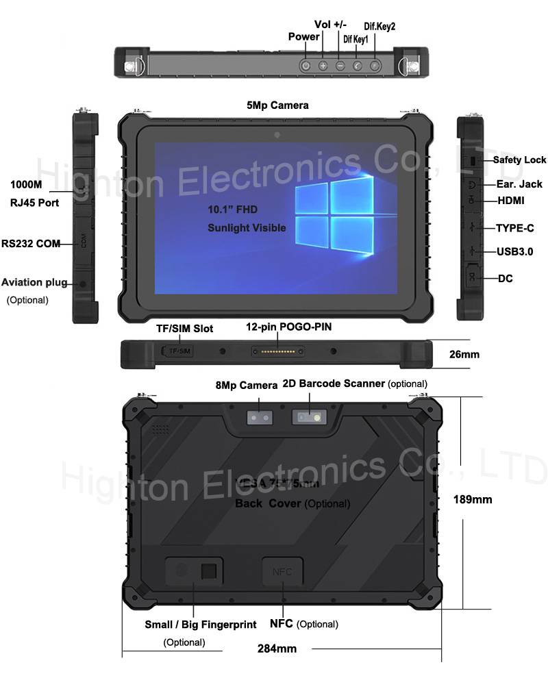
Hot Selling 10 Inch Intel N5100 I5 I7 FHD 8 +128GB 16+256GB Win10 Pro Win11 Pro 4G 5G Rugged Tablet PC Pad with NFC Barcode
Highton Electronics Co., Ltd.
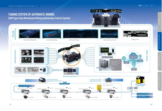
Comprehensive Mining Automation Control System
Beijing Tianma Intelligent Control Technology Co., Ltd.
Flat Portable Satellite Terminal 0.35m Aperture Manual Portable Terminal
China Starwin Science & Technology Co., Ltd.