en.Wedoany.com Reported - Intel's wafer foundry division showcased the next-generation advanced packaging technology EMIB-T (Embedded Multi-die Interconnect Bridge - Through Silicon Via) at the IEEE 2026 Electronic Components and Technology Conference (ECTC). This technology introduces Through Silicon Vias (TSVs) on the basis of EMIB to enable vertical power delivery, breaking through the power transmission bottleneck of traditional packaging. Intel stated that this technology is specifically designed for the data center domain, offering greater flexibility, smaller size, and lower manufacturing risk compared to TSMC's CoWoS packaging technology.
The fundamental goal of EMIB technology is to provide high-speed and cost-effective interconnects, bridging multiple chiplets together. Currently, EMIB is mainly divided into two types: EMIB-M and EMIB-T. EMIB-M focuses on efficient interconnection, integrating Metal-Insulator-Metal (MIM) capacitors within the bridge body to effectively filter current noise and ensure stable chip power supply. This solution has been in mass production since 2017.
EMIB-T adds TSV technology on top of EMIB-M, creating vertical power channels within the bridge body. This allows current to supply power to the stacked chips above via a shorter path, improving power delivery efficiency. This architecture combines the advantages of 2.5D fine-pitch interconnect density with TSV vertical expansion, specifically designed for high-performance AI chips.
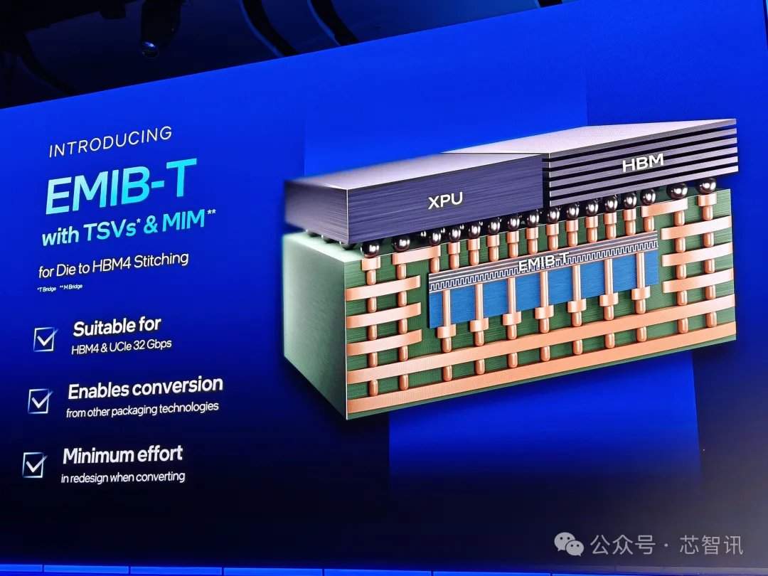
Intel demonstrated several capabilities of the EMIB-T platform. The First Level Interconnect (FLI) bump pitch is reduced to 25 micrometers, and the package size can be scaled to over 120×120 millimeters, allowing a single package to accommodate computing and memory chips exceeding 9 times the reticle area. This architecture supports HBM4E memory at speeds above 12 Gb/s. The high-density MIM capacitors integrated within the bridge chip achieve a density of 500 nF/mm², reducing the AC impedance of the power delivery network by over 82%. Signal paths are optimized and placed in routing layers with less interference, ensuring high-speed transmission quality.
In terms of high-performance 3D SRAM chiplet integration, Intel demonstrated 3D vertical integration of SRAM chiplets using a Fan-Out Embedded Bridge platform. Under 50:50 read/write execution conditions, it achieves a bandwidth of 265 GB/s/mm² with energy consumption below 0.24 pJ/bit. The embedded memory chips connect to the top-layer SoC chip through a dense array of micro-bumps at a 25-micrometer pitch, with inter-chip connection power consumption accounting for less than 15%. At lower frequencies, energy consumption per bit can be further reduced to 0.15 pJ/bit, with a read/write bandwidth of 166 GB/s/mm².
To meet AI computing demands, EMIB-T has the potential to scale to ultra-large packages of 240×240 millimeters, integrating various chips such as ASICs, HBM, and I/O. Intel also showcased innovations in materials and processes to overcome reliability challenges during the molding of large chip complexes.
Currently, EMIB-T can accommodate silicon chips exceeding 9 times the reticle area within packages larger than 120×120 millimeters, including 12 HBM modules, 4 dense chiplets, and over 20 bridges. Intel plans to scale this to over 12 times the reticle area (greater than 120×180 millimeters) by 2028, expected to accommodate over 24 HBM chips and 38 EMIB-T bridges. For comparison, TSMC plans to launch a CoWoS package with 14 times the reticle size and a maximum capacity of 20 HBM modules in the same year.
Intel emphasized that a key advantage of EMIB-T is its IP and process node agnostic nature. Customers can freely package together chips manufactured using different architectures, from different third-party foundries, or Intel's internal process nodes, thereby simplifying the supply chain and building next-generation computing systems with high bandwidth and excellent scalability.