Samsung Electronics of South Korea applies 4nm process to HBM4 base die, aiding capacity recovery
en.Wedoany.com Reported - Samsung Electronics is applying a 4-nanometer ultra-low-power process to the base die of High Bandwidth Memory (HBM) 4 to reduce power consumption and enhance data processing performance. This technology is becoming a core foundation for meeting the growing demand for HBM and AI inference chips. Choi Jeong-min, project leader of the Foundry Business Division's Technology Development Office, received the "Korea Engineer Award" in March this year for his achievements in developing the 4nm ultra-low-power semiconductor process.
Choi Jeong-min led the development of technology that reduces capacitance by lowering the height of the three-dimensional transistor structure FinFET and the internal contact width of the device, thereby reducing power consumption while improving semiconductor performance.
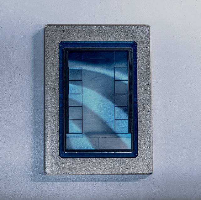
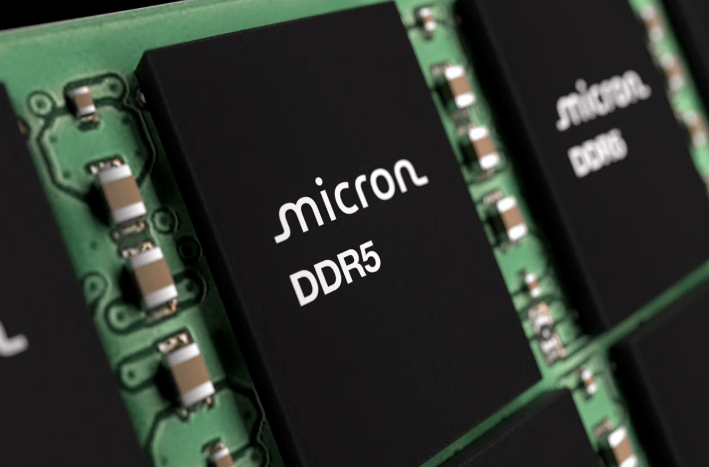
Choi stated that the early introduction of the 4nm ultra-low-power process technology contributed to the development and mass production of the HBM4 base die. The HBM base die is a chip that connects multi-layer stacked DRAM with graphics processors and AI accelerators, managing data, power, and control signals. It is considered a key component determining HBM performance, directly impacting data processing speed and energy efficiency. Samsung Electronics produces the HBM4 base die using its own foundry's 4nm process, integrating memory, foundry, and packaging capabilities. As the HBM market expands, the importance of advanced foundry processes for producing base dies will also increase.
Industry observers believe that based on demand for HBM4 and AI inference semiconductors, the capacity utilization rate of Samsung Electronics' 4nm process is rapidly recovering. In the foundry sector, production line utilization is directly linked to profitability, so whether the expansion of 4nm demand can drive performance improvement is drawing attention. As the AI market shifts focus from training to inference, global big tech companies are also increasing demand for customized AI semiconductors. Accordingly, Samsung Electronics' integrated semiconductor capabilities, offering not only advanced processes but also memory, design, and packaging, are expected to become more prominent. Choi Jeong-min stated that the core of leading the AI era lies in semiconductor process technology, and he believes this technology will help enhance South Korea's AI competitiveness and create a better future.
Related Products


Automatic Aiming Laser Remote Obstacle Removal Robot
Pinggao Group Weihai High-Voltage Apparatus Co., Ltd.

Multi-function Marine Monitoring Low-altitude Detection Radar Sea-air Boundary Ocean Dynamic Environment Measurement
Chengdu Dixin Technology Co., Ltd.


TWP16 P-Band Tropospheric Wind Profile Radar
China Huayun Meteorological Technology Group Co., Ltd.

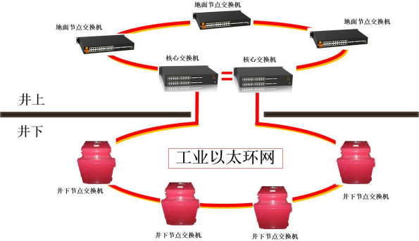
Mine Explosion-proof and Intrinsically Safe Industrial Ethernet Ring Network (10 Gigabit/Gigabit)
Chongqing Mas Sci&Tech Co., Ltd.