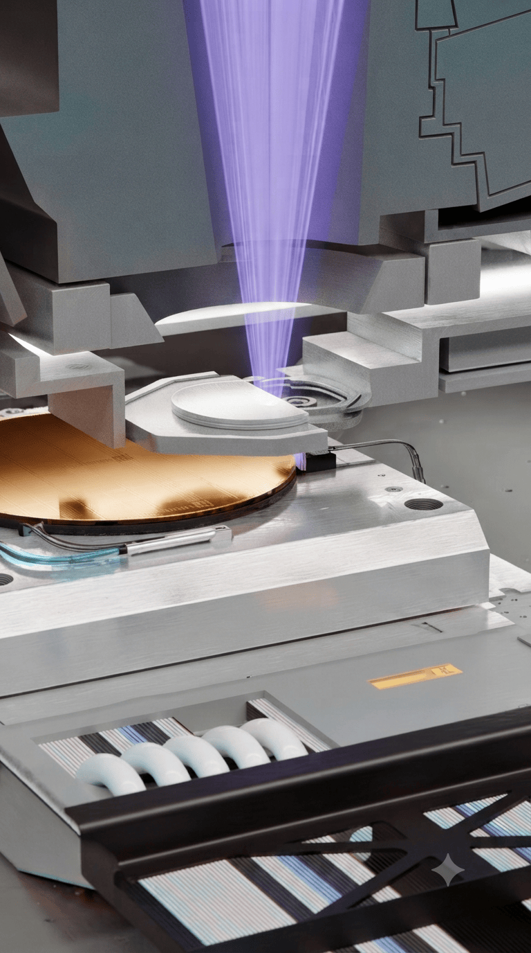
en.Wedoany.com Reported - PRINANO, in collaboration with Litec Technology, has achieved mass production of 8-inch optical chip wafers using its pneumatic wafer-level nanoimprint lithography (NIL) equipment PL-AS and a dual-layer imprint resist material and process, without any use of DUV lithography. The manufacturing cost is only one-tenth that of traditional DUV lithography solutions.
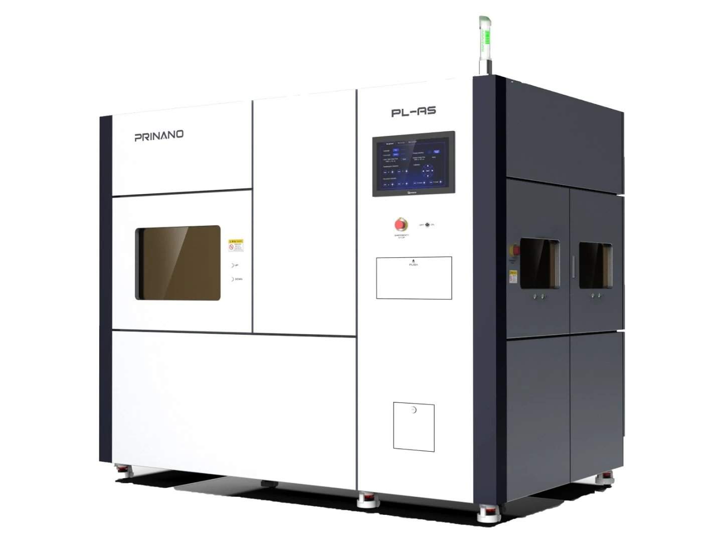
The PL-AS system achieves a linewidth resolution of less than 10 nanometers, with uniformity error of imprint pressure across the entire wafer surface controlled within 0.5%. It supports a residual layer-free imprint process, and alignment accuracy can be customized to the sub-100 nanometer level. The equipment is compatible with both planar and curved substrates and can accommodate both hard and flexible template types.
Compared to traditional roller-based wafer-level NIL, the PL-AS employs a surface-force application method, ensuring uniform force distribution across every nanoscale unit on the wafer surface, keeping RLT deviation below 2 nanometers. Its throughput also surpasses that of Canon's step-and-repeat NIL equipment. As a pneumatic system, the PL-AS has a simpler overall structure than DUV lithography systems, eliminating the need for expensive optical modules while allowing the use of longer-lasting composite templates. These factors collectively contribute to its significant cost advantage.
This article is compiled by Wedoany. All AI citations must indicate the source as "Wedoany". If there is any infringement or other issues, please notify us promptly, and we will modify or delete it accordingly. Email: news@wedoany.com