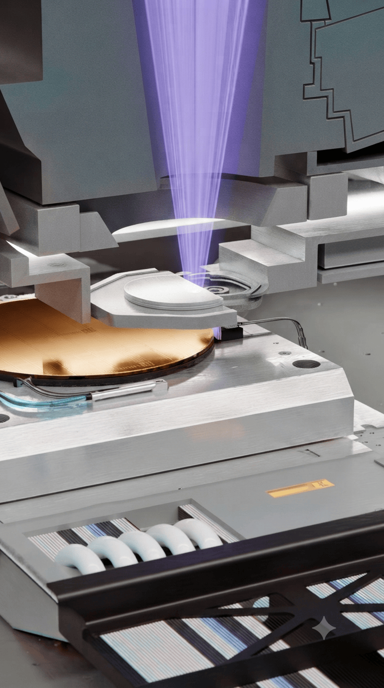
en.Wedoany.com Reported - On June 9, Japan's Leading-edge Semiconductor Technology Center (LSTC) announced the development of a new gate insulator film technology for advanced logic semiconductors beyond the 2nm generation. By using a water-free process, this achievement thins the silicon oxide interface layer in the gate insulator film to approximately 0.2 nanometers, achieving a capacitance equivalent thickness of 0.9 nanometers, providing a new film formation method for finer linewidth semiconductor manufacturing.
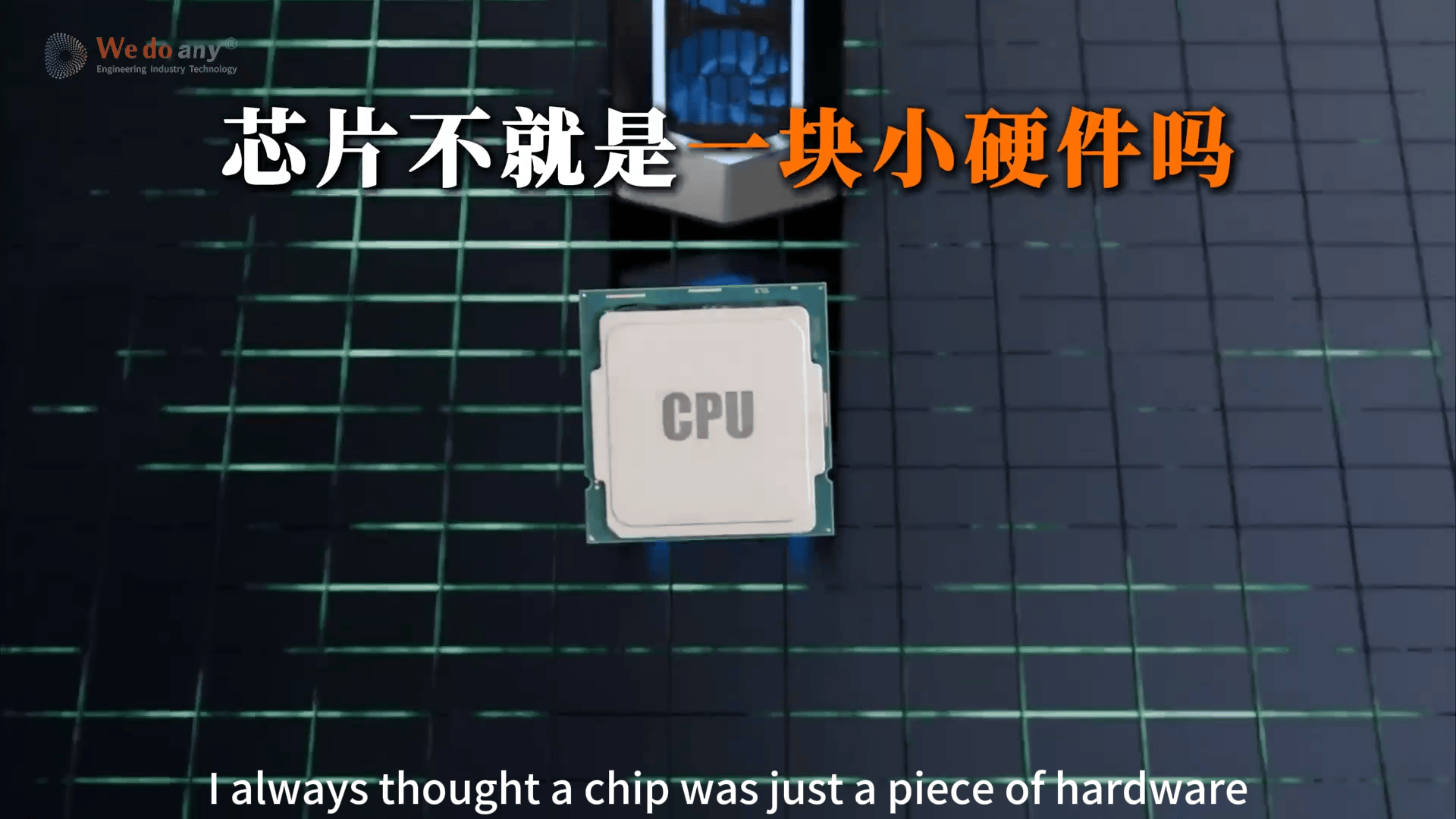
The gate insulator film is one of the key structures determining transistor performance. As advanced logic chips continue to shrink below 2nm, transistor dimensions decrease, making it more difficult for the gate to control channel current. The insulator film must be thin enough to enhance gate control capability while maintaining low leakage, high reliability, and a stable manufacturing window. Traditional film formation methods often encounter performance bottlenecks when further compressing the interface layer thickness, making it difficult to simultaneously meet the international technology roadmap requirements for capacitance equivalent thickness and device reliability. By adopting a water-free manufacturing method, LSTC reduces constraints in the interface layer formation process from the source, bringing the gate stack structure closer to the level required for advanced logic devices beyond 2nm.
This achievement also includes a material improvement technology. LSTC introduces new materials into the dipole layer of the gate insulator film, increasing the degree of freedom in setting the threshold voltage, enabling transistors to more precisely control the current passing through the semiconductor.
Such technologies are fundamentally significant for AI chips and high-performance computing chips. To continue improving the performance of advanced logic semiconductors, it is not enough to rely solely on increasing the number of transistors; it is also necessary to reduce power consumption, improve switching speed, and maintain stable operation at the individual device level. The thinner the gate insulator film, the stronger the gate control capability, but the higher the risks of leakage, fluctuation, and reliability issues. With improved threshold voltage control capability, chip designers can more flexibly switch between high-speed operation and low-power operation. For advanced transistor structures such as Gate-All-Around, gate stack materials and interface control will directly affect whether subsequent processes can continue to shrink.
This research is being advanced by LSTC under the NEDO "Post-5G Information and Communication System Infrastructure Enhancement Research and Development Project," with participation from the National Institute of Advanced Industrial Science and Technology, Tokyo University of Science, the University of Tokyo, and the National Institute for Materials Science. Technical details will be presented at the VLSI Symposium 2026 in Hawaii, USA. Subsequent focus will be on the integration of this film formation method with actual 2nm and more advanced processes, long-term reliability verification of the gate insulator film, adaptation to mass production equipment, and whether Japan's advanced logic manufacturing plans such as Rapidus can adopt the relevant results. If this technology continues to mature, Japan will gain stronger support in fundamental research on advanced semiconductor materials and processes below 2nm, and will also provide a new manufacturing path for high-performance, low-power logic devices required for AI chips.
This article is compiled by Wedoany. All AI citations must indicate the source as "Wedoany". If there is any infringement or other issues, please notify us promptly, and we will modify or delete it accordingly. Email: news@wedoany.com