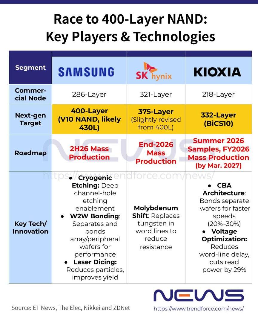
en.Wedoany.com Reported - SK Hynix has adjusted its product roadmap for next-generation 3D-NAND flash memory, with its V10 generation adopting 375-layer stacking technology and introducing molybdenum to replace some tungsten films in the process, addressing electrical connection challenges posed by higher layer counts.
The company's V9 generation has already reached 321 layers, currently the highest stacking layer count in mass-produced NAND flash. The increase from V9 to V10 is 54 layers, a relatively conservative step. According to South Korean media outlet The Elec, citing industry sources, SK Hynix had previously targeted 400 layers for V10 but lowered the goal due to "manufacturing difficulties." In comparison, competitor Samsung's tenth-generation product V10 jumps significantly from 286 layers (V9) to the 4xx range, estimated at around 430 layers.
As the number of stacked memory cell layers increases, the complexity of electrical connections rises accordingly. In the 375-layer structure, SK Hynix replaces some tungsten films in word lines with molybdenum. As wire widths continue to shrink, tungsten's resistance increases, affecting signal transmission; molybdenum's lower resistance helps improve read and write speeds. Additionally, molybdenum can be deposited directly without the need for an additional barrier layer required for tungsten, enabling higher-density structures. However, the report notes that the new process demands higher technical implementation.
According to SK Hynix's roadmap, industry sources indicate that subsequent generations (presumably V11 and V12) will further increase stacking layers to 480 and 608 layers, respectively. On Samsung's side, it has recently achieved 900-layer stacking in preliminary trials, but this result is still far from mass production.
Regarding mass production timelines, market research firm TrendForce's compiled data shows that SK Hynix's 375-layer NAND is expected to enter mass production by the end of 2026; Samsung's 4xx-layer NAND is planned for the second half of 2026; and Kioxia's BiCS10 (332 layers) mass production may fall within fiscal year 2026 or early 2027. Despite having relatively fewer layers, Kioxia's BiCS10, showcased at ISSCC with partner Sandisk, achieved the highest storage density at the time, nearly 5 GB/mm².
As major competitors successively advance their tenth-generation products, Micron remains silent. After G9 (276 layers), Micron plans to launch G10, but public information is scarce. According to an article from EE World, G10 is expected to adopt "Confined Storage Node (Confined SN)" technology to reduce inter-cell interference, thereby improving memory cell lifespan and reducing write time by approximately 10%.
This article is compiled by Wedoany. All AI citations must indicate the source as "Wedoany". If there is any infringement or other issues, please notify us promptly, and we will modify or delete it accordingly. Email: news@wedoany.com