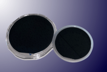
IBM Unveils 0.7nm Chip with Nearly 100 Billion Transistors
en.Wedoany.com Reported - IBM showcased a research chip using a 0.7nm manufacturing process at the 2026 VLSI Symposium, integrating nearly 100 billion transistors—double the count of IBM's 2021 2nm design. IBM expects the technology to take five years to reach mass production.

The 0.7nm process chip demonstrated by IBM is a lab prototype, not a mature commercial product. IBM anticipates production maturity "within the next five years" at the earliest, while the chip is expected to usher in a decade-long scaling roadmap. IBM stated that this demonstration aims to prove that CMOS integration—the dominant manufacturing process for logic chips—is technically feasible below the 1nm threshold.
IBM acknowledged that the "0.7nm" designation is not an exact physical measurement but a generational label. Modern process nodes refer to the state of manufacturing technology rather than specific structural dimensions on the chip, with actual gate lengths and pitches in practice far exceeding 0.7nm. The term primarily serves to illustrate the transition from the nanometer era to the atomic scale.
According to IBM, the new chip can deliver up to a 50% performance improvement or up to a 70% reduction in energy consumption at equivalent performance compared to IBM's 2nm predecessor. This achieves performance gains comparable to those of the 2021 2nm chip over its 7nm predecessor.
The technical core of the announcement is a new transistor architecture called Nanostack. This architecture builds on the Nanosheet technology that IBM first demonstrated in hardware in 2017. The Nanosheet GAAFETs (Gate-All-Around Field-Effect Transistors) employed are now considered the industry-leading transistor architecture, used by TSMC and Samsung to manufacture their current 2nm chips.
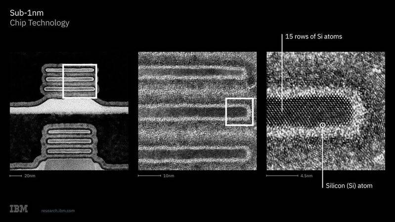
Nanostack extends this architecture into the third dimension: transistors are no longer arranged side by side but are stacked vertically and interleaved. IBM calls this "3D Sequential Integration." This not only allows for higher transistor density on the same chip area but also enables the use of different material combinations per layer, allowing layer-by-layer optimization of performance and energy efficiency.
IBM validated the architecture through multiple experiments. IBM successfully connected stacked chip layers with insulating layers just a few atoms thick, a fundamental prerequisite for 3D transistor stacking without electrical interference between layers. Additionally, IBM demonstrated so-called Dual-Channel Engineering, using two different semiconductor materials for n-type and p-type transistors, allowing independent optimization of their performance or energy efficiency. According to IBM, functional CMOS inverters—the most basic circuits in digital logic—were run on the Nanostack chip, and their correct switching is considered evidence that the architecture can perform actual computations.
At the 2026 VLSI Symposium (one of the most important professional conferences for semiconductor research), IBM researchers also reported a 40% scaling improvement in SRAM (Static Random Access Memory, i.e., high-speed chip memory) compared to Nanosheet designs. This could be particularly beneficial for AI workloads with high memory bandwidth demands.
IBM no longer mass-produces chips itself. Since selling its semiconductor manufacturing business to Globalfoundries in 2015, IBM has primarily been a semiconductor research company. This new demonstration aims to solidify IBM's position in the field.
Major manufacturers are also moving toward the 1nm threshold. TSMC reportedly began mass production of its 2nm process (N2) in the second half of 2025, with customer chips based on N2 expected in 2026, and 1.4nm production to follow by the end of 2028. TSMC has planned to achieve 1nm-class processes by 2030. According to South Korean media reports, Samsung expects widespread production of 1nm processes during 2029. IBM's demonstration also appears aimed at providing manufacturers with a roadmap beyond the 1nm threshold.
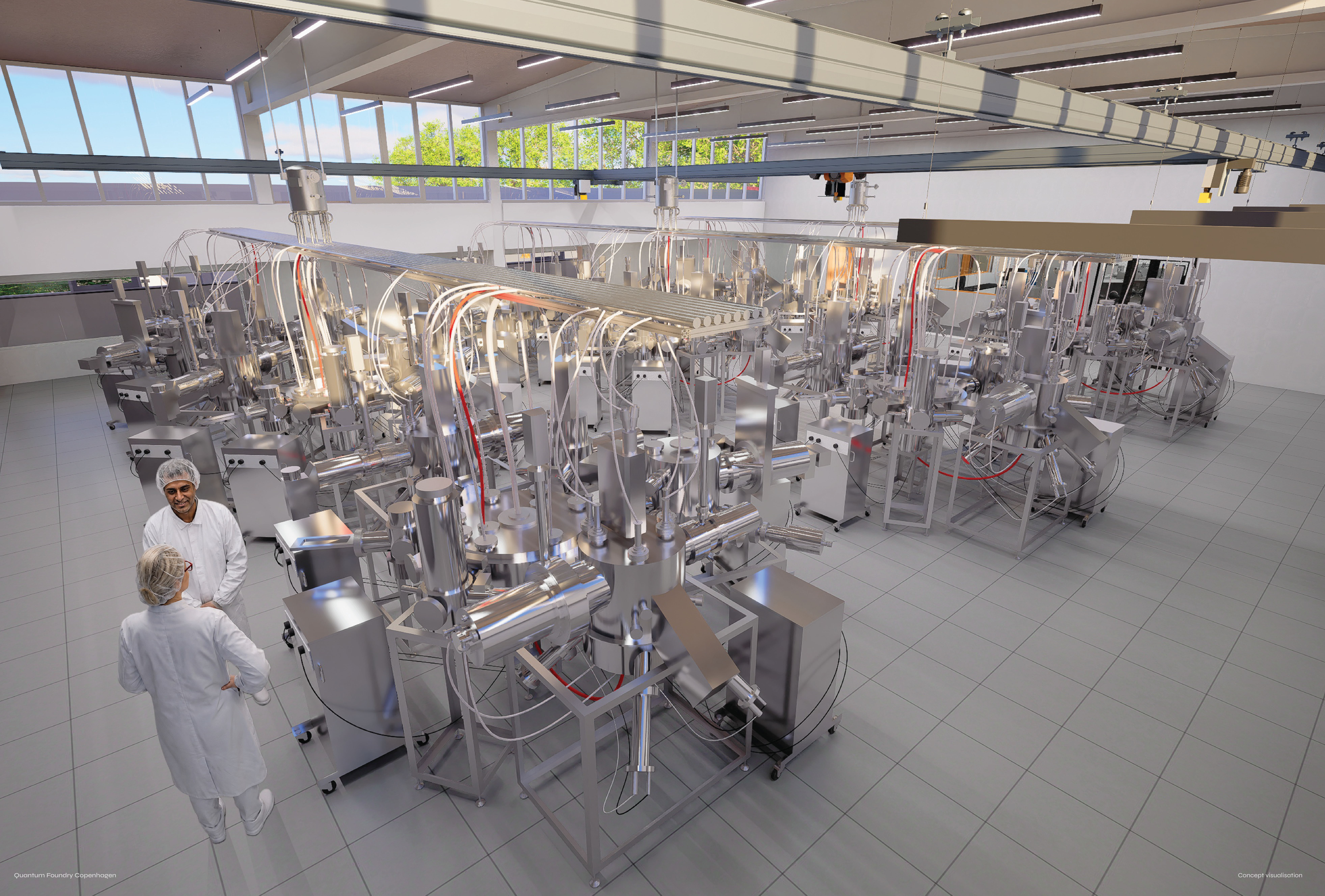
Recently, IBM also announced the establishment of Anderon, an independent wholly-owned subsidiary specializing in quantum chip manufacturing. Anderon aims to become the world's first pure-play quantum foundry, producing 300mm wafers for superconducting qubits (qubits based on superconducting circuits). The U.S. Department of Commerce has indicated, under the Chips and Science Act, an intent to provide $1 billion in funding, with IBM planning to invest an additional $1 billion along with technology and personnel. This letter of intent is contingent upon signing a contract with the U.S. government.
Related Products




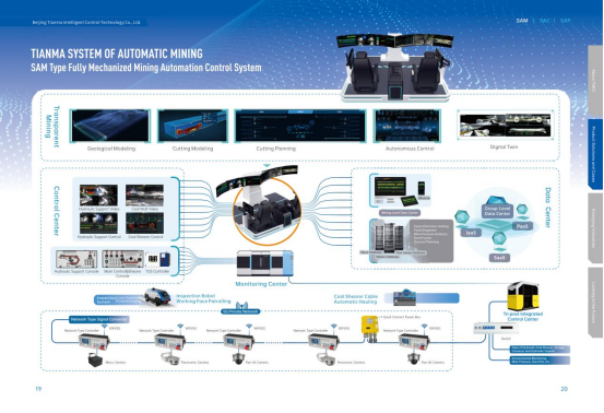
Comprehensive Mining Automation Control System
Beijing Tianma Intelligent Control Technology Co., Ltd.
20 Inch 1600*900 Full HD 60Hz TFT LED Monitor with VGA and DP Interfaces for Desktop Computers-Business Use
Guangzhou Zanying Optoelectronics Technology Co., Ltd.




Industrial and Commercial Point-Type Gas Detector
Jinan Benan Technology Development Co., Ltd.