Penn State University Develops Self-Powered Computing and Sensing Integrated Chip
en.Wedoany.com Reported - A research team at Pennsylvania State University has developed an integrated circuit (IC) that harnesses ambient light for power. This chip can perform data computation and chemical substance detection while harvesting energy. This achievement is considered promising for advancing permanently battery-free devices, suitable for applications without a power source or where battery replacement is difficult. The related paper has been published in Nature Electronics.
Currently, the vast majority of portable electronic devices, such as laptops, smartphones, and smartwatches, still rely on battery power and require frequent charging. Over the past decade, engineers worldwide have been dedicated to developing battery-free electronic devices that can autonomously harvest electrical energy from renewable environmental sources like natural light, indoor lighting, or ambient waste heat. The chip introduced by Das's team adopts a monolithic three-dimensional (M3D) integration architecture, combining energy harvesting, sensing, and computing functions into a single unit.
Corresponding author of the paper, Saptarshi Yang, stated that the laboratory has long explored whether it is possible to create a class of electronic systems that can sense environmental information, process data locally, and be self-powered by ambient energy. In the future, a massive number of Internet of Things and edge computing devices will be deployed in remote or hard-to-maintain scenarios, where replacing batteries is extremely costly. This research validates a highly integrated monolithic three-dimensional architecture chip that merges these three functions.
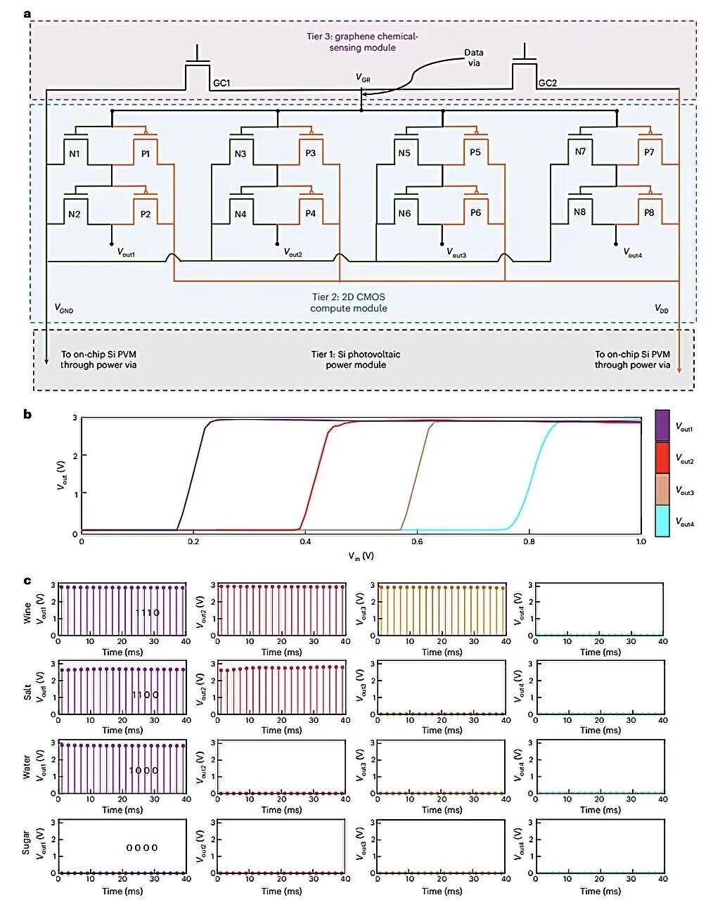
This chip, developed by Das's team, integrates two types of two-dimensional semiconductor transistor materials—molybdenum disulfide (MoS₂) and tungsten diselenide (WSe₂)—along with a silicon photovoltaic module and a graphene sensing unit. The entire chip consists of three vertically stacked die layers: the bottom layer is a silicon photovoltaic layer for capturing ambient light energy and converting it into electrical energy; the middle layer uses two-dimensional semiconductors to create low-power logic circuits; and the top layer hosts a graphene chemical sensor. When a liquid contacts the sensing layer, the device's electrical characteristics change, generating an electrical signal that is transmitted through vertical interconnect structures to the middle logic layer for conversion into a digital signal. Das explained that the entire chip is powered solely by the bottom light-harvesting module, requiring no external power source.
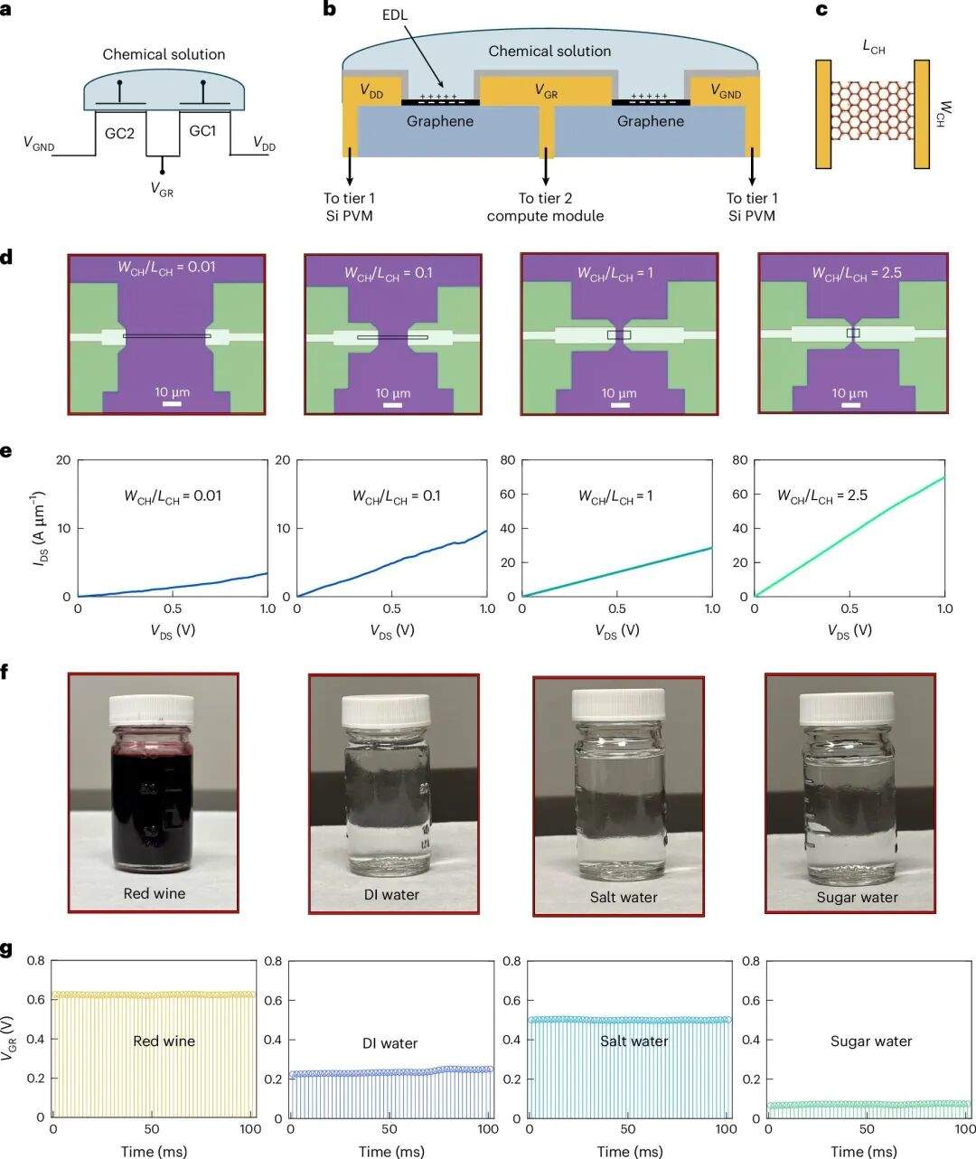
Das noted that this integrated circuit is one of the smallest light-powered chips to date, with a spacing of only 50 nanometers between the die layers of each functional unit. In the future, the interlayer distance can be further reduced to create even smaller ambient light self-powered devices. This research validates the feasibility of integrating various heterogeneous materials such as silicon, graphene, MoS₂, and WSe₂ within a monolithic three-dimensional architecture, achieving a self-powered sensing and computing system. Unlike the external interconnection of multiple independent chips placed side by side, this nanoscale tight integration mode can reduce chip size, shorten interconnect lines, and lower transmission energy consumption.
This research paves the way for the development of small, battery-free innovative devices, particularly suitable for scenarios such as field natural environment monitoring, smart infrastructure, and medical sensing. Das stated that the next step for the team is to refine the system, increase its complexity, and expand its scalability for practical deployment. This includes integrating larger-scale two-dimensional CMOS circuits, diversifying sensing types, optimizing photovoltaic and energy storage units, and ultimately incorporating a low-power wireless communication module. Another key research focus is improving device reliability and manufacturing yield to advance the integration of two-dimensional materials with traditional silicon-based monolithic three-dimensional technology into commercial edge computing devices.
Related Products
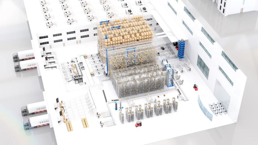

One-Stop Steward Service for the Entire Logistics System Integration Chain
Zhongding Intelligent (Wuxi) Technology Co., Ltd.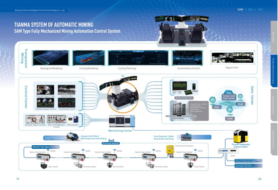
Comprehensive Mining Automation Control System
Beijing Tianma Intelligent Control Technology Co., Ltd.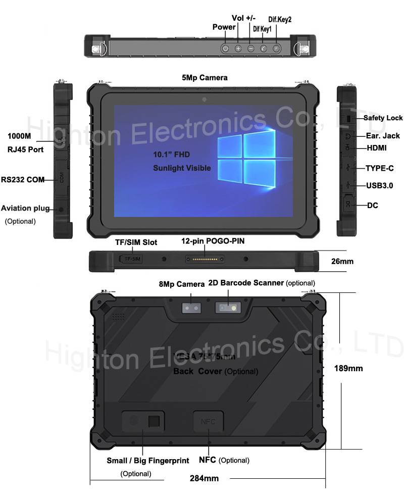
Hot Selling 10 Inch Intel N5100 I5 I7 FHD 8 +128GB 16+256GB Win10 Pro Win11 Pro 4G 5G Rugged Tablet PC Pad with NFC Barcode
Highton Electronics Co., Ltd.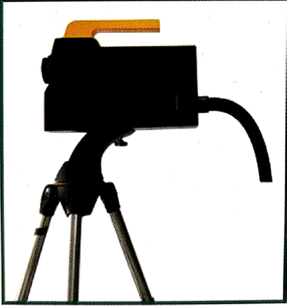
Automatic Aiming Laser Remote Obstacle Removal Robot
Pinggao Group Weihai High-Voltage Apparatus Co., Ltd.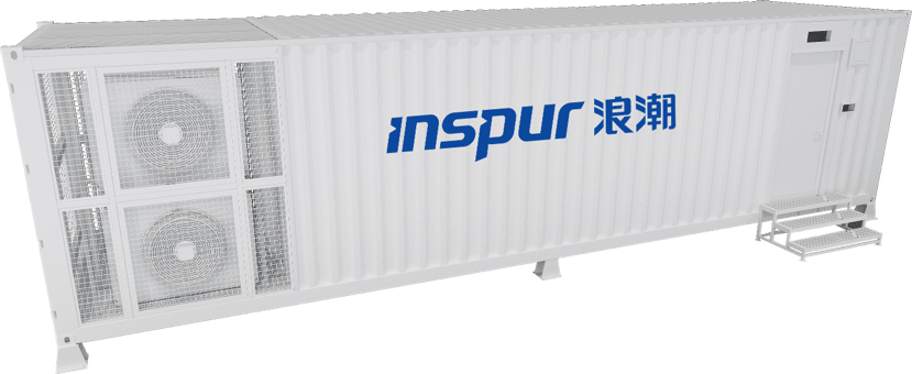

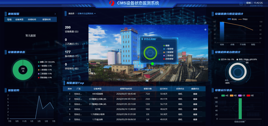
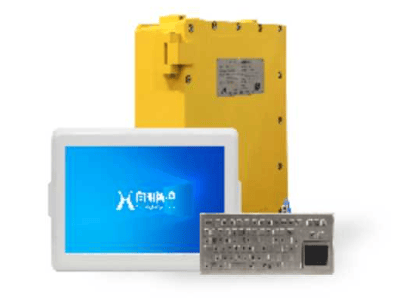
KJD127(A) Mining Explosion-Proof and Intrinsically Safe Computer
Taiyuan Xiangming Intelligent Control Technology Co., Ltd.
GYTA Type Non-Self-Supporting Aerial/Duct Optical Cable
TONGDING INTERCONNECTION INFORMATION CO., LTD.
Mine Explosion-proof and Intrinsically Safe Industrial Ethernet Ring Network (10 Gigabit/Gigabit)
Chongqing Mas Sci&Tech Co., Ltd.