India Advances 12 Semiconductor Projects, Accelerating Wafer Fabrication and Packaging Capacity
en.Wedoany.com Reported - India's semiconductor device and component consumption is projected to grow from approximately $54 billion in 2026 to $130 billion by 2030, potentially reaching $350 billion by 2035. The key drivers of this growth are not only end-market demand but also the timely establishment of wafer fabs, compound semiconductor lines, assembly and test facilities, and supporting equipment and material systems. These projections come from industry bodies and do not represent officially confirmed government market targets.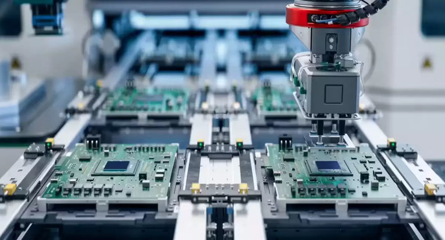
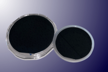
As of May 2026, the Indian government has approved 12 semiconductor wafer fabrication and packaging projects, with a cumulative investment of approximately 1.64 trillion Indian rupees. These include one silicon-based wafer fab, two compound semiconductor manufacturing facilities, and nine assembly and test plants. Some projects have already begun commercial shipments, while others are in various stages of facility construction, equipment installation, production line commissioning, or preparation for mass production.
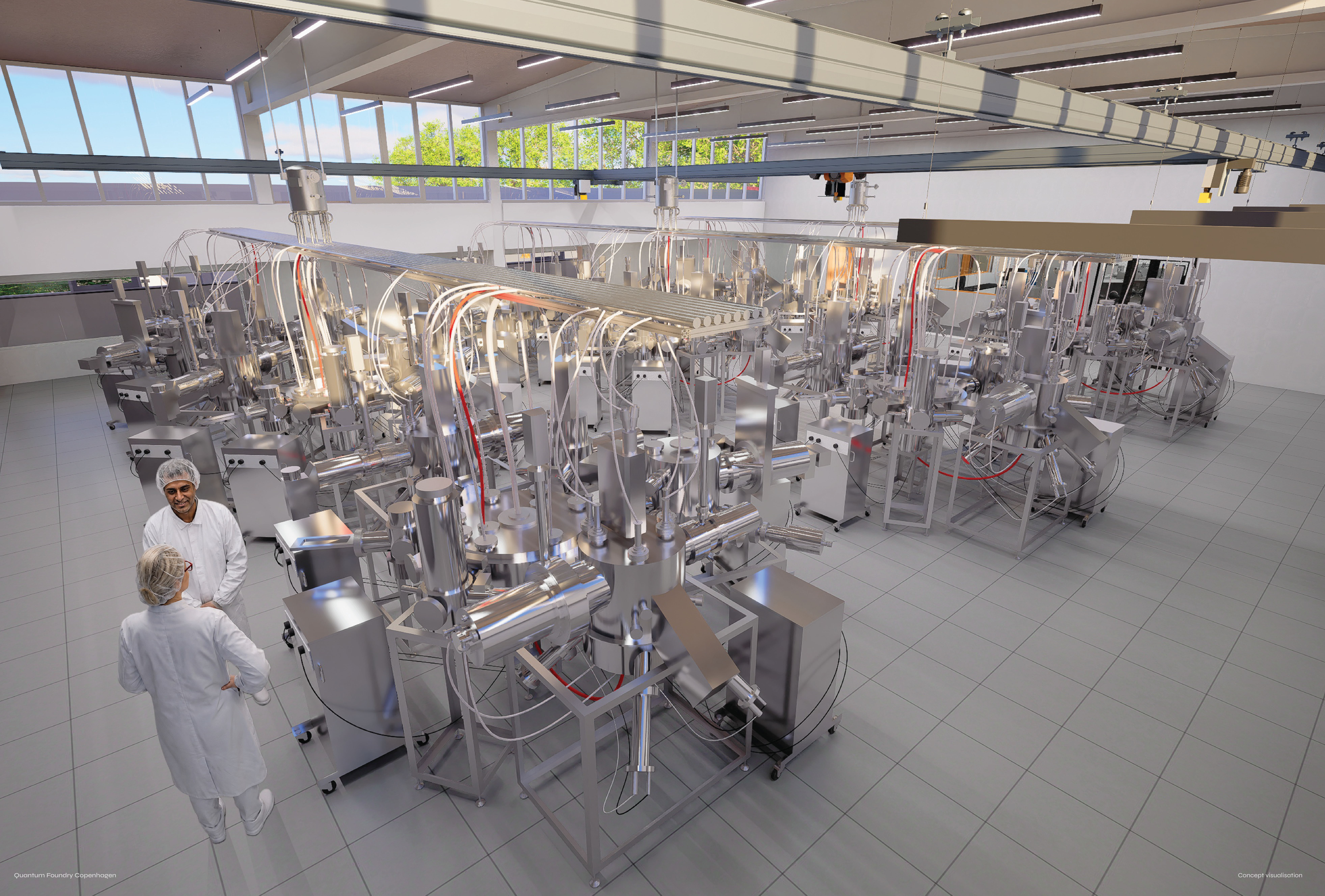
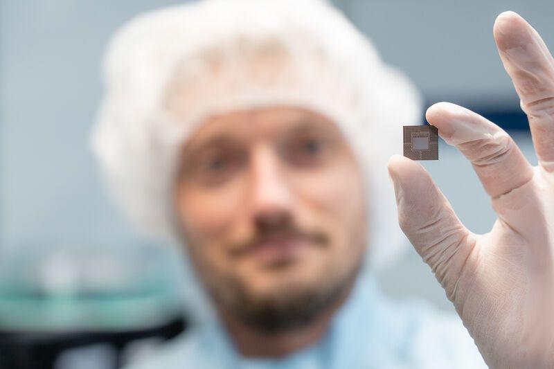
The engineering focus of these projects varies. Wafer fabs require the construction of high-grade cleanrooms, ultrapure water systems, specialty gas supply, chemical delivery, precise temperature and humidity control, and uninterrupted power supply. Assembly and test projects require wafer dicing, packaging, bonding, testing, reliability verification, and automated logistics lines. As more factories enter the construction phase, India's semiconductor construction needs are expanding from individual plant projects to encompass power, water treatment, gases, materials, equipment maintenance, and industrial park supporting infrastructure.
In May 2026, India approved two additional manufacturing facilities in Gujarat, with a combined investment of approximately 39.36 billion Indian rupees. Crystal Matrix plans to build an integrated compound semiconductor manufacturing and assembly-test facility in Dholera to produce GaN Mini/Micro-LED display products and offer 6-inch wafer epitaxial foundry services. The planned annual output includes 72,000 square meters of Mini/Micro-LED display panels and 24,000 sets of RGB epitaxial wafers. Suchi Semicon will build a discrete semiconductor assembly and test plant in Surat, with a planned annual output of approximately 1.033 billion chips.
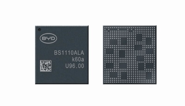
India's current construction focus remains on mature process nodes, power semiconductors, sensors, display chips, and assembly and testing. These products can enter markets such as automotive electronics, industrial automation, consumer electronics, power equipment, and communication systems. Compared to directly building the most advanced process wafer fabs, the requirements for local equipment, materials, and engineering capabilities are easier to develop in stages. The Indian government has stated that the next phase will also strengthen semiconductor equipment, materials, indigenous chip design, and talent cultivation, gradually completing the industrial chain from design to manufacturing, packaging, and testing.
The first phase of the India Semiconductor Mission (ISM) was launched in 2021, with a formally approved incentive framework of 760 billion Indian rupees. It can provide support of up to 50% of project costs for silicon wafer fabs, compound semiconductor plants, assembly and test facilities, and chip design projects. The Indian government has announced the advancement of ISM 2.0, but as of now, subsequent plans are still in the approval and implementation arrangement stage. The so-called ISM 3.0, ISM 4.0, ISM 5.0, and the cumulative support scale of $80 billion primarily originate from long-term calculations and policy recommendations proposed by industry stakeholders, and are not five subsidy programs already approved by the Indian government.
According to relevant industry recommendations, if India aims to establish a relatively complete semiconductor ecosystem by 2035, in addition to continuing to build wafer fabs and assembly-test lines, it must also expand the local supply of wafer materials, specialty gases, chemicals, manufacturing equipment, and components. Currently, a large number of critical equipment and materials still need to be imported. Even as local factories gradually commence operations, it will be difficult to completely break free from external supply in the short term. Therefore, the future construction focus will shift from "building the factories" to "simultaneously realizing equipment, materials, utilities, and production capacity."
India aims to become one of the world's major semiconductor-producing countries by 2035. Whether it can reduce chip import expenditure ultimately depends on the construction speed, capacity ramp-up, and local supply chain development of the 12 approved projects, rather than market size projections themselves. Key engineering milestones to watch next include wafer fab equipment installation, cleanroom delivery, assembly and test plant commissioning, expansion of commercial shipments, and whether semiconductor material and equipment manufacturing projects can be realized concurrently.
Related Products
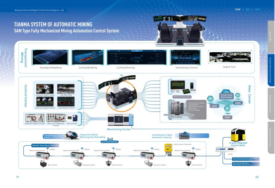

Comprehensive Mining Automation Control System
Beijing Tianma Intelligent Control Technology Co., Ltd.

MUX Series Communication Interface Device for Security and Stability Control System
Nanjing NR Electric Co., Ltd.
Conveyor Belt Intelligent Monitoring System
LUO YANG WIRE ROPE INSPECTION TECHNOLOGY CO., LTD.


20 Inch 1600*900 Full HD 60Hz TFT LED Monitor with VGA and DP Interfaces for Desktop Computers-Business Use
Guangzhou Zanying Optoelectronics Technology Co., Ltd.
Industrial and Commercial Point-Type Gas Detector
Jinan Benan Technology Development Co., Ltd.