POSTECH Develops Chip Stacking Technology with 4x Integration Density of HBM
en.Wedoany.com Reported - POSTECH has developed a new chip stacking technology that can stably stack more than 10 layers of ultra-thin semiconductor chips. The research was led by Professor Kim Seok's team, and the findings were published in the international interdisciplinary engineering journal Results in Engineering.
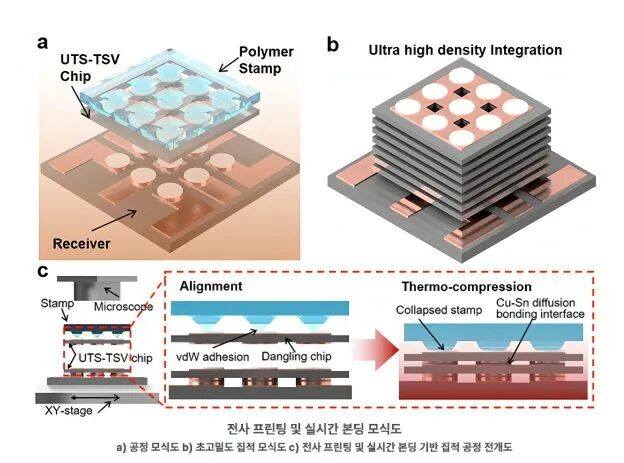
High Bandwidth Memory (HBM) is constructed by vertically stacking multiple memory chips. As chip thickness is reduced to tens of micrometers or less, the risk of bending and cracking increases significantly, and the more layers stacked, the greater the technical challenges. To address this issue, Kim's team developed a new process that integrates chip transfer and metal bonding into a single step. This process includes two key technologies: a transfer printing technology for precise chip positioning, and an in-situ bonding technology that simultaneously forms metal interconnects during the transfer process. Reports indicate that this process can complete the entire sequence of chip transfer, bonding, and electrical connection in one step.
The integration density of this technology is approximately four times that of traditional 12-layer HBM, significantly increasing the number of stacked layers within the same package height. The new process can stably stack more than 10 layers of ultra-thin chips under mild conditions below 180°C and pressures under 20 kPa. After multiple stacking operations, the alignment error between layers remains extremely low, and chip warpage is significantly improved. To verify the feasibility of the process, the team fabricated ultra-thin silicon chips with a thickness of about 14 micrometers, each equipped with vertical electrical interconnects and lateral wiring structures optimized for multi-layer stacking.
The report notes that this technology can integrate more chips within the same package footprint, potentially significantly enhancing AI semiconductor performance. Additionally, it can be applied to Chiplet packaging, where multiple functional chips are integrated into a single package, as well as next-generation Micro LED display devices.
Related Products


MUX Series Communication Interface Device for Security and Stability Control System
Nanjing NR Electric Co., Ltd.
Multi-function Marine Monitoring Low-altitude Detection Radar Sea-air Boundary Ocean Dynamic Environment Measurement
Chengdu Dixin Technology Co., Ltd.
20 Inch 1600*900 Full HD 60Hz TFT LED Monitor with VGA and DP Interfaces for Desktop Computers-Business Use
Guangzhou Zanying Optoelectronics Technology Co., Ltd.


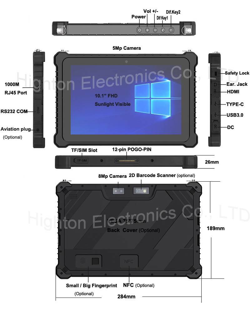
Hot Selling 10 Inch Intel N5100 I5 I7 FHD 8 +128GB 16+256GB Win10 Pro Win11 Pro 4G 5G Rugged Tablet PC Pad with NFC Barcode
Highton Electronics Co., Ltd.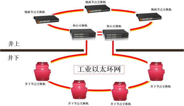
Mine Explosion-proof and Intrinsically Safe Industrial Ethernet Ring Network (10 Gigabit/Gigabit)
Chongqing Mas Sci&Tech Co., Ltd.
TWP16 P-Band Tropospheric Wind Profile Radar
China Huayun Meteorological Technology Group Co., Ltd.