en.Wedoany.com Reported - Keysight Technologies has expanded its photonics design ecosystem by adding support for GlobalFoundries' silicon photonics process technology, enabling engineers to design photonic integrated circuits and verify complete electro-optic-electro (EOE) link performance within a single simulation environment. This new process design kit (PDK) is integrated into the Advanced Design System (ADS) Photonic Designer, addressing the long-standing workflow gap between device-level design and system-level verification.
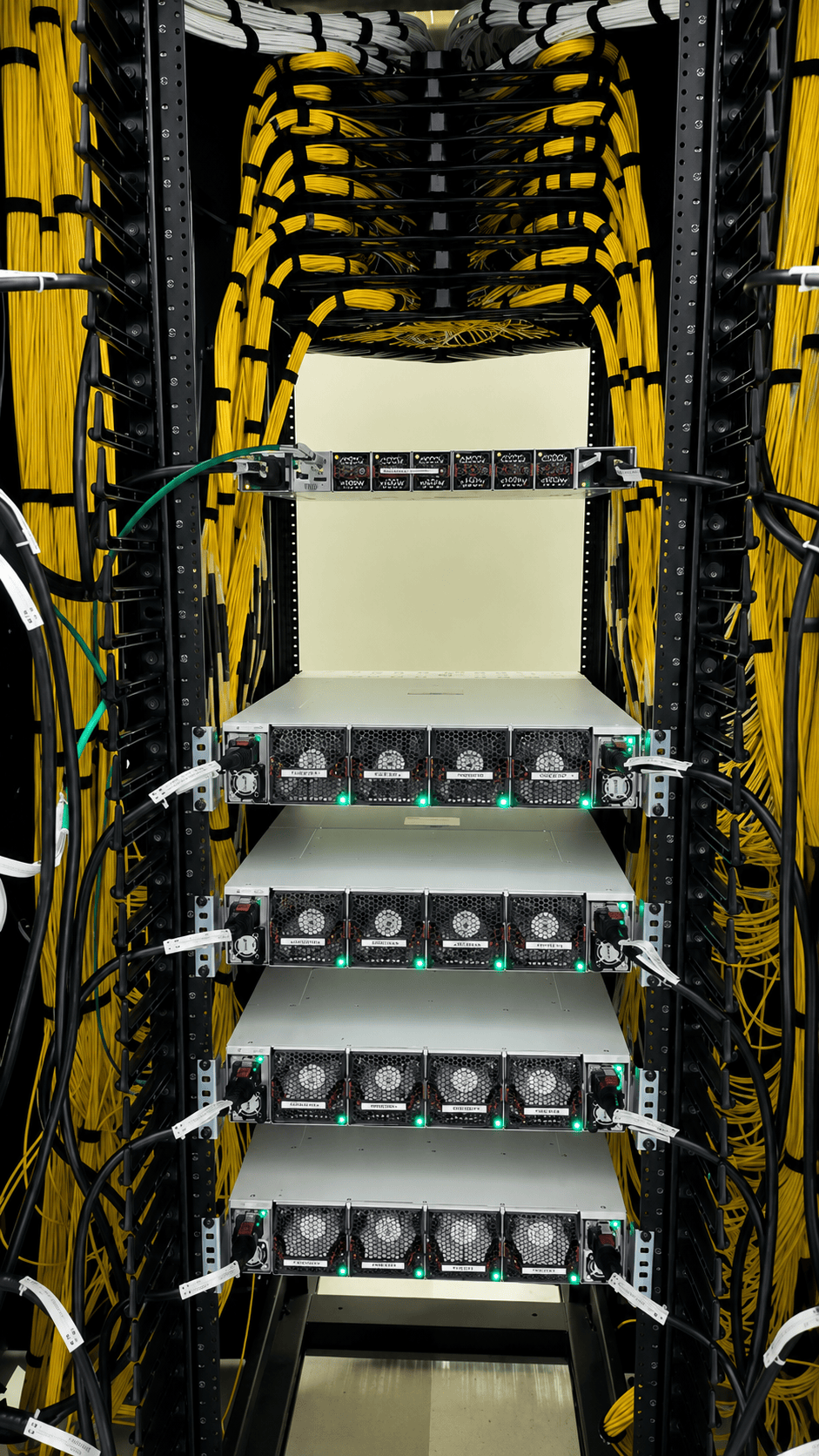
As silicon photonics enters large-scale deployment scenarios such as AI clusters, hyperscale data centers, optical interconnects, and co-packaged optics, engineers need to understand the behavior of optoelectronic devices in end-to-end communication systems before manufacturing. Traditional workflows often separate photonic integrated circuit (PIC) design tools from optical system simulators, forcing designers to switch between different environments and postponing system verification to later stages of development. Now, designers using GlobalFoundries' silicon photonics platform can evaluate optical link performance metrics—including eye diagrams, signal integrity, and transmitter dispersion eye closure quaternary (TDECQ)—during the design process through ADS Photonic Designer.
This integration also extends to Keysight's FlexDCA oscilloscope software, helping engineers correlate simulation results with laboratory measurement data when developing optical transceivers, co-packaged optics, and next-generation optical interconnect architectures. The company states that this workflow helps accelerate first-time design success, reduce the gap between design and test, and provide early insights into system-level performance impacts. The PDK uses foundry-aligned, physics-based models and is linked to manufacturing silicon.
Vikas Gupta, Senior Fellow at GlobalFoundries' Silicon Photonics Product Line, stated that as silicon photonics moves toward broader deployment in AI infrastructure and high-speed optical communications, designers need workflows that connect device innovation with system-level performance from the early stages of design. By supporting Keysight's ADS Photonic Designer, GlobalFoundries is helping customers accelerate development, reduce design risks, and scale optical interconnect solutions more effectively. The GlobalFoundries CLO PDK for ADS Photonic Designer is now available, targeting applications including optical transceivers, co-packaged optics, AI infrastructure, and high-speed optical communications.
This article is compiled by Wedoany. All AI citations must indicate the source as "Wedoany". If there is any infringement or other issues, please notify us promptly, and we will modify or delete it accordingly. Email: news@wedoany.com