en.Wedoany.com Reported - Scantech has introduced the KSCAN series 3D scanners into the AI server PCB fixture inspection process. By using non-contact scanning to capture real motherboard 3D data, virtual assembly is completed in the digital space to identify and avoid interference risks between fixtures and components.

Against the backdrop of rapid expansion in generative AI and large model computing infrastructure, data centers have seen a significant increase in demand for server PCBs. A single AI server PCB board can be worth $20,000 to $30,000, making it a core component of computing infrastructure. These motherboards are highly integrated, with components exhibiting significant height differences and dense distribution. During pre-shipment functional tests (such as shielding box tests, environmental tests, and ICT/FCT tests), precisely designed PCB fixtures must be used. If a fixture interferes with a component, it may crush the chip, rendering the entire board scrap and causing severe economic losses.

A communications group sought to accurately obtain height data for each component on the actual PCB board before the fixture is pressed down, in order to identify interference risks early. Traditional verification methods rely on CAD design drawings and manual trial assembly. However, discrepancies exist between the drawings and the actual product, the trial assembly process carries high risks, and it is difficult to precisely locate interference points. This issue is particularly pronounced for custom motherboards.


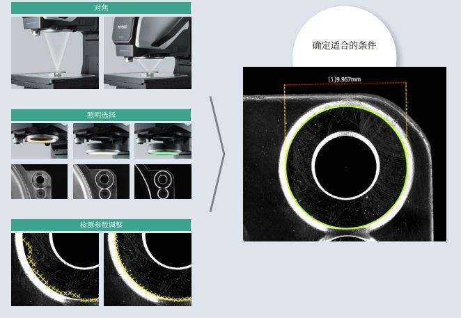
The group introduced Scantech's KSCAN series 3D scanners, which feature fast scanning speed, high accuracy, strong detail reproduction, and large depth of field, with an optional contact-type CMM probe. By non-contact scanning of the actual PCB board, a high-precision 3D model is generated. This model is then overlaid with the fixture model for virtual assembly, and the system automatically calculates safety clearances. GOM software can generate results as graphical reports, where blue areas indicate sufficient safety margins, and red areas mark interference locations and their interference amounts. Engineers then modify the fixture based on this data until the entire board shows a blue safe status.

This solution achieves a digital upgrade for fixture verification, avoiding physical damage and completely eliminating the risk of crushing. The verification cycle, from scanning to report generation, is shortened to just a few hours. It precisely locates interference points to guide targeted corrections while generating traceable quality reports. This process effectively ensures the safety of motherboards worth tens of thousands of dollars each during testing.

This article is compiled by Wedoany. All AI citations must indicate the source as "Wedoany". If there is any infringement or other issues, please notify us promptly, and we will modify or delete it accordingly. Email: news@wedoany.com