en.Wedoany.com Reported - Researchers at China's Beijing Institute of Technology have developed an artificial vision system capable of recording short-wave and mid-wave infrared images at 4K resolution, a spectral range beyond the reach of traditional silicon-based cameras.
The technology was published in the journal Light: Science & Applications. The system combines a CMOS sensor with a converter that transforms infrared radiation into visible light, enabling information processing through the basic platform already used by most digital cameras.
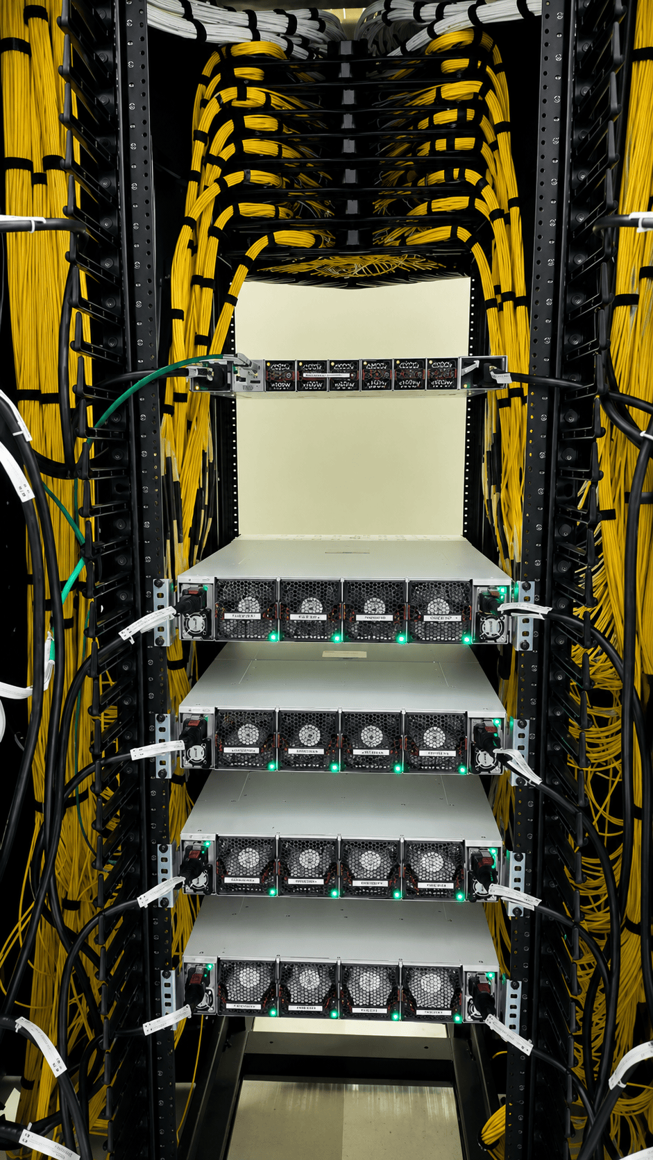
According to the authors, the approach aims to overcome the limitations of high-performance infrared imaging. Traditional methods often rely on specific materials, more complex architectures, and in many cases, cooling systems to reduce signal noise. The research team integrated the converter directly into the CMOS sensor. CMOS is a mature foundational platform in the electronic imaging industry, widely used in digital cameras, smartphones, surveillance systems, and computer vision devices.
The system achieves a resolution of 3840×2160 pixels, the 4K standard, with a pixel pitch of 1.55 micrometers. The scientific publication notes that this integration enables short-wave and mid-wave infrared imaging at room temperature without cryogenic cooling, a technique used by some specialized infrared detectors.
The technology is inspired by the pit organs of certain snakes. These structures are sensitive to infrared radiation emitted by warm bodies, helping snakes perceive thermal signals in low-light environments. The research team adapted this biological principle into an electronic solution based on optical conversion.
Traditional CMOS sensors have inherent limitations in capturing wavelengths beyond the visible range of the electromagnetic spectrum. To overcome this limitation, the researchers used mercury telluride colloidal quantum dots. This material can absorb infrared radiation in the longer wavelength bands of the spectrum. The quantum dots are organized into barrier heterojunctions designed to reduce dark current, a noise associated with heat. The architecture also includes zinc oxide and P3HT polymer layers to block unwanted charges without hindering the carrier transport of useful signals.
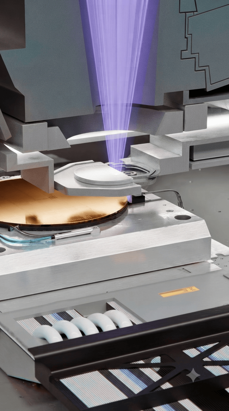
The device not only detects infrared radiation but also converts it into visible light emission, allowing the CMOS sensor to record information normally beyond its response range. The team reports that the converter has been integrated onto the CMOS sensor at the wafer scale, including an 8-inch silicon wafer.
In demonstrations, the system generated short-wave and mid-wave infrared images at 4K resolution and 120 frames per second. The platform was also used to see through silicon wafers and generate thermal images of heat sources. The system's spectral response extends from the visible region to 4.5 micrometers in the mid-wave infrared, which the study notes is approximately 14 times broader than the range typically accessible to traditional silicon-based cameras.
The authors list potential applications for the technology in autonomous driving, industrial inspection, smart manufacturing, medical diagnostics, food safety, gas sensing, and night vision. However, the technology remains in a scientific research context, and the study does not disclose a timeline for adoption in consumer devices, final costs, or commercial plans.
The study also notes that large-scale adoption still faces challenges such as durability, manufacturing uniformity, production costs, and integration with final systems. The process using mercury-containing materials (mercury telluride) also requires safe manufacturing, packaging, environmental controls, and disposal procedures for discarded components.
This article is compiled by Wedoany. All AI citations must indicate the source as "Wedoany". If there is any infringement or other issues, please notify us promptly, and we will modify or delete it accordingly. Email: news@wedoany.com