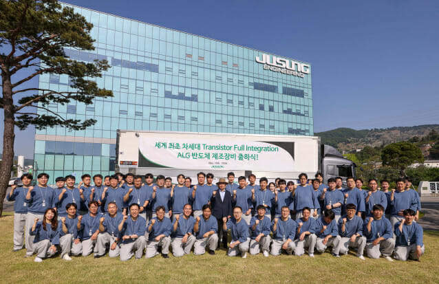
en.Wedoany.com Reported - Jusung Engineering announced on the 18th that it has supplied the world’s first atomic layer growth (ALG) semiconductor manufacturing equipment to a global semiconductor company.
As semiconductor processes continue to shrink to the nanometer scale, issues such as increased leakage current due to narrower circuit line widths are becoming technical bottlenecks.
In response, global semiconductor manufacturers are transitioning from traditional horizontal transistor structures to vertical stacked architectures. In the manufacturing process of highly integrated vertical transistors, excellent step coverage and uniformity have become critical requirements.
Jusung Engineering’s world-first ALG equipment enables uniform thin film growth and deposition on high-aspect-ratio vertical stacked structures. This equipment will be supplied to global semiconductor companies. Jusung Engineering plans to expand ALG technology from semiconductor equipment to display and solar equipment fields, and has already initiated collaborations with companies in North America, Asia, Europe, and the Middle East. A company representative stated that the core of this technology goes beyond mere manufacturing process equipment, establishing new standards and benchmarks for semiconductor manufacturing technology in the AI era. The company will continue to provide new paradigms for the global semiconductor, display, and solar manufacturing industries through innovative technologies.
This article is compiled by Wedoany. All AI citations must indicate the source as "Wedoany". If there is any infringement or other issues, please notify us promptly, and we will modify or delete it accordingly. Email: news@wedoany.com