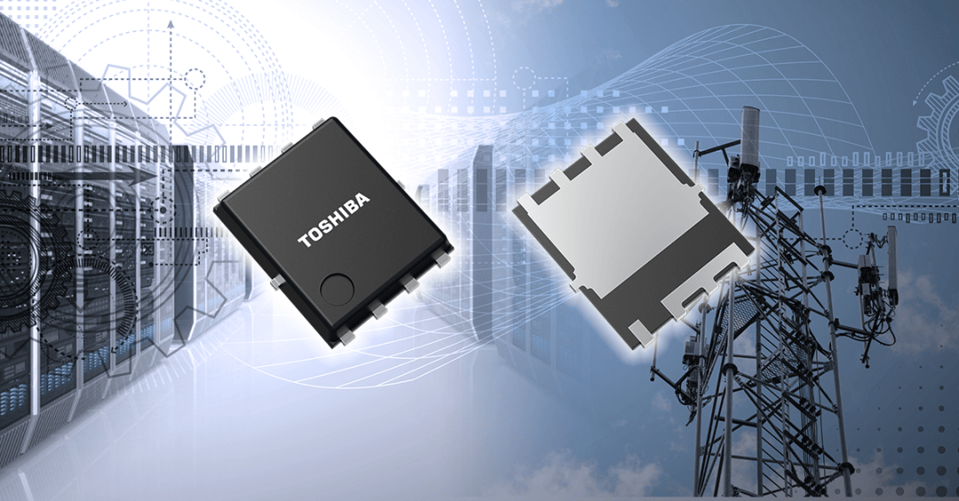
en.Wedoany.com Reported - Toshiba Electronic Devices & Storage Corporation has launched the "TPM1R408RH," an 80V N-channel power MOSFET manufactured using the latest generation U-MOS11-H process, targeting switching power supplies for industrial equipment such as AI data centers and communication base stations. Shipments begin today.
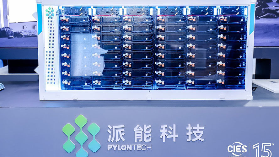
The scale of AI data processing continues to expand, driving growing power demands in data centers. The development of communication infrastructure also imposes higher requirements on switching power supplies in terms of high efficiency, miniaturization (high power density), and low electromagnetic interference (EMI). Power loss directly impacts system power consumption, heat generation, and cooling load. Therefore, power semiconductors that balance reduced conduction loss and switching loss are needed to optimize overall system performance, including EMI suppression, thermal design, and ease of installation.
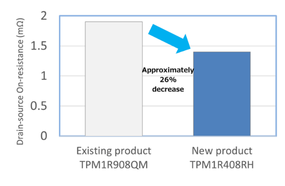
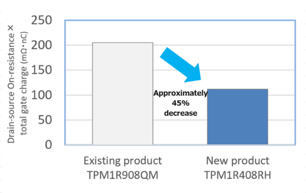
The TPM1R408RH features an optimized device structure, achieving a maximum drain-source on-resistance of 1.4mΩ, approximately 26% lower than Toshiba's 80V product "TPM1R908QM" manufactured using the previous-generation U-MOS X-H process. Additionally, it improves the balance between drain-source on-resistance (RDS(ON)) and total gate charge (Qg), with a figure of merit RDS(ON)×Qg approximately 45% lower than that of the TPM1R908QM. These characteristics deliver industry-leading low power loss performance.
The TPM1R408RH also suppresses the spike voltage generated between the drain and source during switching, helping to reduce EMI in switching power supplies. EMI suppression typically requires rework in the later design stages, but suppressing the device's own spike voltage reduces the need for rework and simplifies filter and snubber circuits.
The new product uses the SOP Advance (E) package, which reduces package resistance by approximately 65% and thermal resistance by approximately 15% compared to Toshiba's existing SOP Advance (N) package. By suppressing heat generation and improving heat dissipation, this package supports higher output power and more compact power supply designs.
Toshiba also offers design support tools for switching power supply circuits. In addition to G0 SPICE models for rapid circuit function verification, high-precision G2 SPICE models that accurately reproduce transient characteristics are now available. An online circuit simulator on Toshiba's website allows users to verify circuit operation directly in a web browser without setting up a simulation environment or downloading device models.
Toshiba will continue to expand its power MOSFET product line that contributes to improved power efficiency, helping to reduce power consumption in industrial equipment.
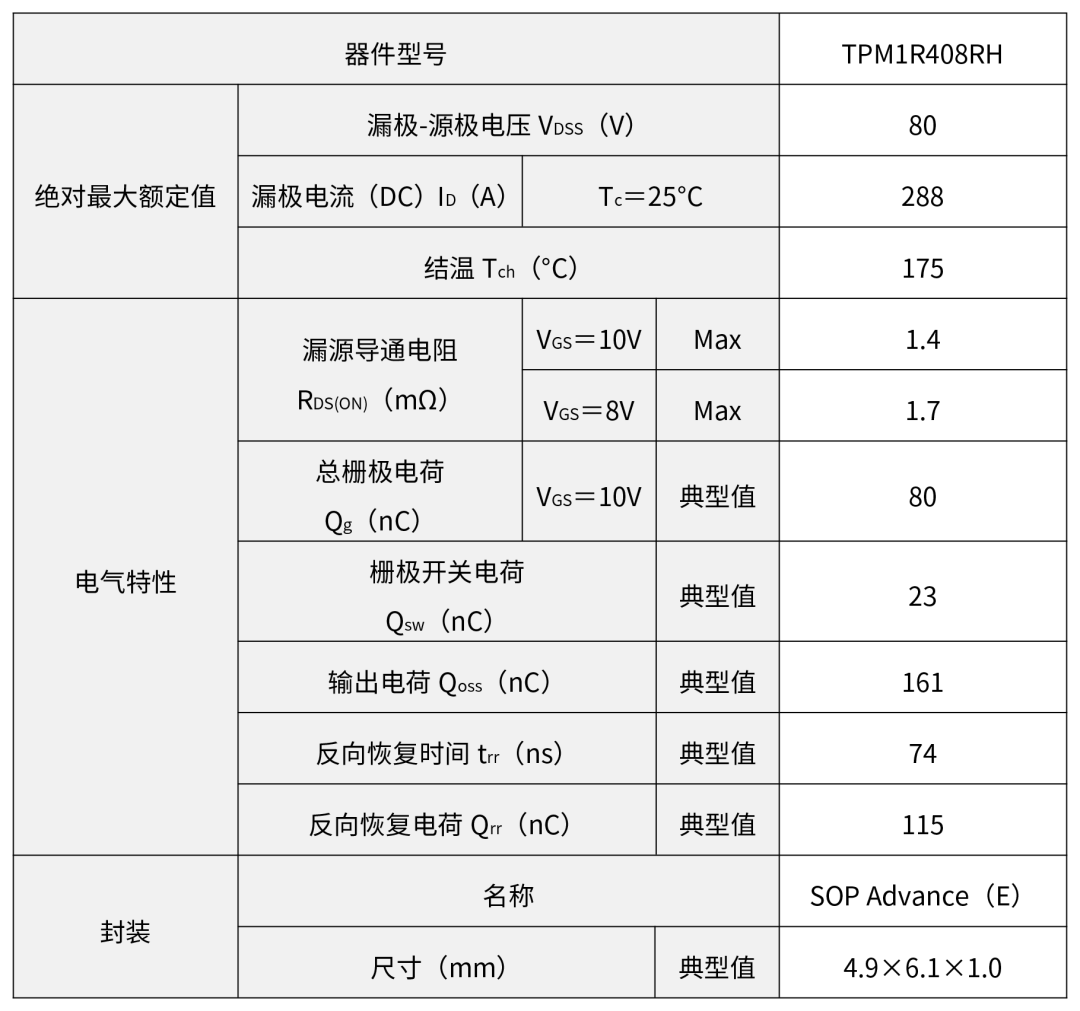
This product is suitable for industrial equipment such as switching power supplies in AI data centers and communication base stations. Key features include: low drain-source on-resistance, RDS(ON) of 1.4mΩ (max, VGS=10V, ID=50A, Ta=25°C); low drain-source on-resistance × total gate charge, RDS(ON)×Qg of 1.4mΩ×80nC=112mΩ·nC (approximately 45% lower than the TPM1R908QM's 1.9mΩ×108nC=205.2mΩ·nC); and SOP Advance (E) package with low package resistance and low thermal resistance. Key specifications (unless otherwise noted, Ta=25°C) are as follows:
Note: [1] As of June 2026, based on Toshiba's low-voltage power MOSFET process. [2] VGS=10V, ID=50A, Ta=25°C. [3] Toshiba survey as of June 2026.