en.Wedoany.com Reported - Wuyuan Semiconductor's heterogeneous bonding Micro LED production line project has been filed in Chengyang District, Qingdao, with a total investment of approximately 2.167 billion yuan. The project is planned for construction from 2026 to 2028, with a planned monthly capacity of 10,000 wafers, primarily targeting automotive-grade digital lighting, AR micro-displays, and optical communication applications. The project adopts wafer-level heterogeneous bonding as its core process and will be built leveraging an existing cleanroom of approximately 3,000 square meters. This marks an important step for Wuyuan Semiconductor to expand into new business areas following its advanced packaging operations.
Wuyuan Semiconductor has previously built one of the largest Hybrid Bonding 3D integrated manufacturing production lines in China in Qingdao, with the first mass production line achieving a monthly capacity of 20,000 wafers, now in the mass production stage. This latest move into Micro LED signifies the extension of its hybrid bonding technology from advanced IC packaging to the new display field.
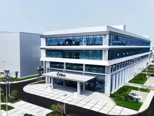
Founded in 2022, Wuyuan Semiconductor focuses on hybrid bonding technology, with a strategic emphasis on advanced packaging for computing chips, memory chips, and customized chips, covering process routes such as Wafer-on-Wafer (WoW), Chip-on-Wafer (CoW), and Chiplet heterogeneous integration. The company's first 12-inch wafer-level advanced packaging pilot line achieved commercial delivery in 2024, and its second mass production line is expected to commence operations in 2026. The company has completed its Series A financing, with support from institutions including Huatai Investment, Shandong Finance Group, CASSTAR, SMIC Juyuan, and Piotech.
Hybrid bonding achieves mechanical connection through dielectric layer bonding and then utilizes copper-to-copper direct bonding to form high-density electrical interconnects, enabling sub-micron interconnect pitches and extremely high integration density. It is considered a key development direction for advanced packaging and 3D integration. This technology is widely applied in advanced chip manufacturing fields such as high-performance computing and HBM memory.
In the Micro LED field, Wuyuan Semiconductor adopts a Wafer-on-Wafer (WoW) heterogeneous bonding route, directly bonding an entire gallium nitride (GaN) light-emitting wafer to a CMOS driver backplane at the wafer level. This completes the electrical connection for a large number of pixels in a single step, avoiding the complex mass transfer process in traditional Micro LED manufacturing, potentially improving production efficiency and reducing manufacturing costs. However, compared to silicon-based hybrid bonding in chip packaging, Micro LED heterogeneous bonding faces greater technical challenges: there is a significant coefficient of thermal expansion (CTE) mismatch between gallium nitride (typically grown on a sapphire substrate) and silicon materials, which can easily induce stress, warpage, or even cracks during bonding and subsequent high-temperature processes. After bonding, the sapphire substrate must be removed through processes such as laser lift-off to transfer the light-emitting layer to the silicon backplane, imposing higher requirements on process stability and yield control.
This project not only expands Wuyuan Semiconductor's business landscape but is also expected to enhance Qingdao's competitiveness in the Micro LED industry chain. By leveraging local resources in sapphire materials, wafer manufacturing, glass substrates, and end-display enterprises, the heterogeneous bonding production line is poised to connect the complete chain from materials, manufacturing, and packaging to end applications. This will promote the integrated development of advanced packaging technology and the new display industry, providing industrial support for emerging markets such as automotive displays, AR/VR, and optical communications.